08.13.15
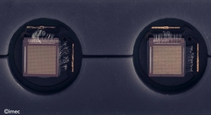
Imec is extending its Gallium Nitride-on-Silicon (GaN-on-Si) R&D program, and is now offering joint research on GaN-on-Si 200mm epitaxy and enhancement mode device technology.
The extended R&D initiative includes exploration of novel substrates to improve the quality of the epitaxial layers, new isolation modules to increase the level of integration, and the development of advanced vertical devices. Imec welcomes new partners interested in next generation GaN technologies and companies looking for low-volume manufacturing of GaN-on-Si devices to enable the next generation of more efficient and compact power converters.
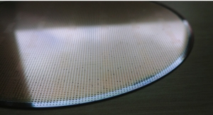
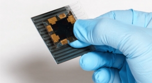
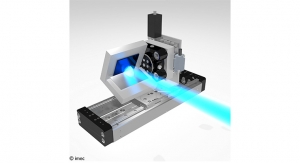
GaN technology offers faster switching power devices with higher breakdown voltage and lower on-resistance than silicon, making it an outstanding material for advanced power electronic components. Building on imec’s track record in GaN epi-layer growth, new device concepts and CMOS device integration, imec has now developed a complete 200mm CMOS-compatible GaN process line.
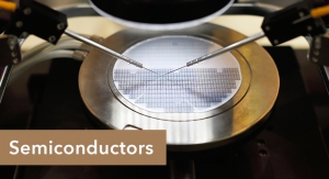
Imec’s GaN-on-Si technology is reaching maturity, and companies can gain access to the platform by joining imec’s GaN-on-Si industrial affiliation program (IIAP). The process line is also open to fabless companies interested in low-volume production of GaN-on-Si devices tailored to their specific needs, through dedicated development projects.
“Since the program’s launch in July 2009, we have benefited from strong industry engagement, including participation from IDMs, epi-vendors and equipment and material suppliers,” said Rudi Cartuyvels, EVP of smart systems at imec. “Imec’s open innovation model allows companies to have early access to next-generation devices and power electronics processes, equipment and technologies and speed up innovation at shared cost.”
The extended R&D initiative includes exploration of novel substrates to improve the quality of the epitaxial layers, new isolation modules to increase the level of integration, and the development of advanced vertical devices. Imec welcomes new partners interested in next generation GaN technologies and companies looking for low-volume manufacturing of GaN-on-Si devices to enable the next generation of more efficient and compact power converters.
GaN technology offers faster switching power devices with higher breakdown voltage and lower on-resistance than silicon, making it an outstanding material for advanced power electronic components. Building on imec’s track record in GaN epi-layer growth, new device concepts and CMOS device integration, imec has now developed a complete 200mm CMOS-compatible GaN process line.
Imec’s GaN-on-Si technology is reaching maturity, and companies can gain access to the platform by joining imec’s GaN-on-Si industrial affiliation program (IIAP). The process line is also open to fabless companies interested in low-volume production of GaN-on-Si devices tailored to their specific needs, through dedicated development projects.
“Since the program’s launch in July 2009, we have benefited from strong industry engagement, including participation from IDMs, epi-vendors and equipment and material suppliers,” said Rudi Cartuyvels, EVP of smart systems at imec. “Imec’s open innovation model allows companies to have early access to next-generation devices and power electronics processes, equipment and technologies and speed up innovation at shared cost.”