10.19.15
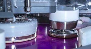
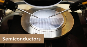
Applied Materials announced it plans to establish a new R&D laboratory in Singapore in collaboration with the Agency for Science, Technology and Research (A*STAR). The S$150 million joint investment will focus on developing advanced semiconductor technology to fabricate future generations of logic and memory chips.
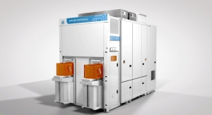
The S$150 million joint lab will be housed within A*STAR’s new R&D cluster at Fusionopolis Two and will feature a 400 square meter Class 1 cleanroom with state-of-the-art semiconductor process equipment that has been custom designed and built by Applied Materials. The facility will be staffed by 60 researchers and scientists, working together with extended research teams at A*STAR’s other research institutes.
The joint lab combines Applied Materials’ expertise in materials engineering, while A*STAR’s will contribute to research in low-defect processing, ultra-thin film materials, materials analysis and characterization, and modeling and simulation in many areas. The intention is for products developed by the joint lab to be manufactured by Applied Materials in Singapore.
“A*STAR and the government of Singapore have been great R&D partners for Applied Materials,” said Gary Dickerson, president and CEO of Applied Materials. “We are excited to expand our collaboration to develop advanced semiconductor technology for extending Moore’s Law.”
“The new joint lab takes the longstanding collaboration between Applied Materials and A*STAR to the next level, and will marshal our combined strengths in research, development, innovation and industrial applications,” added Prof Raj. Thampuran, managing director for A*STAR. “This technology will pioneer new processes and techniques to advance the fabrication of semiconductor devices.”