12.11.15
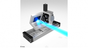
At the IEEE IEDM conference, imec demonstrated record enhancement of novel InGaAs Gate-All-Around (GAA) channel devices integrated on 300mm silicon and explores emerging tunnel devices based on optimization of the same III-V compound semiconductor.
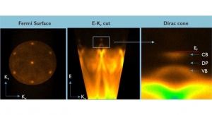
III-V-on-Si GAA devices with a record peak transconductance at 0.5V has been achieved by optimizing both the channel epitaxy quality and the gate-channel passivation. In search of device technologies beyond FinFETs and GAA-nanowires for sub-0.5V operations, imec investigates InGaAs Tunnel-FET (TFETs). homo-junction III-V TFETs achieving a record ON-state current (ION) and superior subthreshold swing have been demonstrated. These results pave the way to advanced logic devices based on III-V-On-Si for high performance or ultra-low power applications.
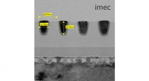
One of the directions that imec is following looks into beyond-Si solutions, such as integrating high-mobility materials into the channels of CMOS devices to increase their performance, and the integration challenges of these materials with silicon. Gate-All-Around Nanowire (GAA NW) FETs have been proven to offer significantly better short-channel electrostatics, and quantum-well FinFETs (with SiGe, Ge, or III-V channels) achieving high carrier mobility, are interesting concepts to increase device performance. Tunnel FETs, on the other hand, offering a steeper than 60mV/dec subthreshold swing, are a promising option for ultra-low power applications.
“Imec’s R&D enables Moore’s law beyond the 5nm technology node through three approaches. First, we are tackling the technology challenges to extend silicon CMOS devices towards smaller nodes. At the same time, we research into disruptive heterogeneous solutions for beyond-silicon CMOS devices to increase performance and introduce new functionalities. Lastly, imec pursues emerging beyond-CMOS devices and systems such as spintronics to investigate further functional scaling beyond device-density-driven scaling,” said Aaron Thean, VP and director of imec’s advanced logic R&D program.
III-V-on-Si GAA devices with a record peak transconductance at 0.5V has been achieved by optimizing both the channel epitaxy quality and the gate-channel passivation. In search of device technologies beyond FinFETs and GAA-nanowires for sub-0.5V operations, imec investigates InGaAs Tunnel-FET (TFETs). homo-junction III-V TFETs achieving a record ON-state current (ION) and superior subthreshold swing have been demonstrated. These results pave the way to advanced logic devices based on III-V-On-Si for high performance or ultra-low power applications.
One of the directions that imec is following looks into beyond-Si solutions, such as integrating high-mobility materials into the channels of CMOS devices to increase their performance, and the integration challenges of these materials with silicon. Gate-All-Around Nanowire (GAA NW) FETs have been proven to offer significantly better short-channel electrostatics, and quantum-well FinFETs (with SiGe, Ge, or III-V channels) achieving high carrier mobility, are interesting concepts to increase device performance. Tunnel FETs, on the other hand, offering a steeper than 60mV/dec subthreshold swing, are a promising option for ultra-low power applications.
“Imec’s R&D enables Moore’s law beyond the 5nm technology node through three approaches. First, we are tackling the technology challenges to extend silicon CMOS devices towards smaller nodes. At the same time, we research into disruptive heterogeneous solutions for beyond-silicon CMOS devices to increase performance and introduce new functionalities. Lastly, imec pursues emerging beyond-CMOS devices and systems such as spintronics to investigate further functional scaling beyond device-density-driven scaling,” said Aaron Thean, VP and director of imec’s advanced logic R&D program.