05.01.16
The Fraunhofer Institute for Organic Electronics, Electron Beam and Plasma Technology FEP will be presenting the first micro-OLEDs patterned using electron beam at Booth 1023 during SID Display Week 2016 in San Francisco, CA from May 24-26.
Fraunhofer FEP has years of experience in the field of processing organic semiconductor materials. Scientists here are also developing organic light-emitting diodes (OLEDs) and OLED microdisplays based on organic semiconductors. Currently, techniques and new applications of electron beam technology – an additional area of core expertise at Fraunhofer FEP – are being particularly investigated in the field of organic electronics.
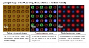
Due to their outstanding optical and electronic properties, OLEDs have a broad range of potential applications in mobile electronics and displays. Small displays with high pixel density, such as OLED microdisplays, are necessary for future applications such as augmented- or virtual-reality, for example. Researchers are now working on further miniaturizing while maintaining high resolution. The patterning of the organic layers in OLEDs represents one of the biggest challenges, as conventional methods such as photolithography cannot be applied to organic semiconductor materials easily.
Fraunhofer FEP scientists have developed a novel approach to pattern the emission area of an OLED at high resolution. The patented technology uses an electron beam process, which takes place after finalizing the OLED including the encapsulation. Therefore it is possible to build the OLED highly productive and completely unpatterned, before the emission is individually modified by an adjusted electron beam process. The energy of the electrons determines their penetration depth in the layer stack. With a suitable choice of process parameters, the encapsulation can also be penetrated by the electron beam and the luminous characteristics of the organic layers beneath will change without destroying or compromising the encapsulation itself. Depending on the application, it is even possible to modify individual layers directly.
“Continuous gray scales in an image can be created on a monochrome OLED using the electron beam, while at the same time the local current consumption is reduced. The longer the dwell time on one spot with the beam, the darker the OLED will appear there,” said Elisabeth Bodenstein from the development team at Fraunhofer FEP.
The process is highly adaptable – regardless of whether the OLED is applied to a rigid medium or flexible film, what color the OLED is, or whether the substrate is optically opaque, translucent or transparent. An enhancement to full-color patterning is being planned.
The Fraunhofer FEP scientists are now prepared to put this new technology into practice with industrial partners. The technology was developed within a project funded by the Fraunhofer Gesellschaft.
Fraunhofer FEP has years of experience in the field of processing organic semiconductor materials. Scientists here are also developing organic light-emitting diodes (OLEDs) and OLED microdisplays based on organic semiconductors. Currently, techniques and new applications of electron beam technology – an additional area of core expertise at Fraunhofer FEP – are being particularly investigated in the field of organic electronics.
Due to their outstanding optical and electronic properties, OLEDs have a broad range of potential applications in mobile electronics and displays. Small displays with high pixel density, such as OLED microdisplays, are necessary for future applications such as augmented- or virtual-reality, for example. Researchers are now working on further miniaturizing while maintaining high resolution. The patterning of the organic layers in OLEDs represents one of the biggest challenges, as conventional methods such as photolithography cannot be applied to organic semiconductor materials easily.
Fraunhofer FEP scientists have developed a novel approach to pattern the emission area of an OLED at high resolution. The patented technology uses an electron beam process, which takes place after finalizing the OLED including the encapsulation. Therefore it is possible to build the OLED highly productive and completely unpatterned, before the emission is individually modified by an adjusted electron beam process. The energy of the electrons determines their penetration depth in the layer stack. With a suitable choice of process parameters, the encapsulation can also be penetrated by the electron beam and the luminous characteristics of the organic layers beneath will change without destroying or compromising the encapsulation itself. Depending on the application, it is even possible to modify individual layers directly.
“Continuous gray scales in an image can be created on a monochrome OLED using the electron beam, while at the same time the local current consumption is reduced. The longer the dwell time on one spot with the beam, the darker the OLED will appear there,” said Elisabeth Bodenstein from the development team at Fraunhofer FEP.
The process is highly adaptable – regardless of whether the OLED is applied to a rigid medium or flexible film, what color the OLED is, or whether the substrate is optically opaque, translucent or transparent. An enhancement to full-color patterning is being planned.
The Fraunhofer FEP scientists are now prepared to put this new technology into practice with industrial partners. The technology was developed within a project funded by the Fraunhofer Gesellschaft.