06.12.17
Silicon-based CMOS (complementary metal-oxide semiconductors) technology has truly shaped our world. It enables most of the electronics that we rely on today, including computers, smartphones and digital cameras.
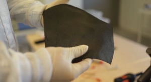
However, to continue the path of progress in the electronics industry new technology must be developed and a key feature of this is the ability to integrate CMOS with other semiconductors. Now, Graphene Flagship researchers from ICFO (The Institute of Photonic Sciences in Barcelona) have shown that it is possible to integrate graphene into a CMOS integrated circuit.
In their paper published in the journal Nature Photonics, they combine this graphene-CMOS device with quantum dots to create an array of photodetectors, producing a high resolution image sensor. When used as a digital camera, this device is able to sense UV, visible and infrared light at the same time. This is just one example of how this device might be used, others include in microelectronics, sensor arrays and low-power photonics.
“The development of this monolithic CMOS-based image sensor represents a milestone for low-cost, high-resolution broadband and hyperspectral imaging systems,” Frank Koppens, ICREA professor at ICFO, noted.
These results were enabled by the collaboration between Graphene Flagship partner Graphenea, a Spanish graphene supplier, and ICFO, within the optoelectronics work package of the Graphene Flagship.
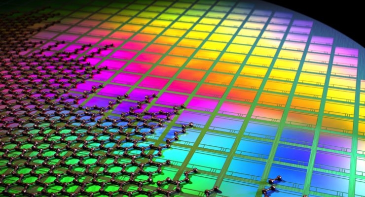
By creating a hybrid graphene and quantum dot system on a CMOS wafer using a layering and patterning approach, the Flagship team solved a complex problem with a simple solution. First the graphene is deposited, then patterned to define the pixel shape and finally a layer of PbS colloidal quantum dots is added.
The photoresponse of this system is based on a photogating effect, which starts as the quantum dot layer absorbs light and transfers it as photo-generated holes or electrons to the graphene, where they circulate due to a bias voltage applied between two pixel contacts. The photo signal is then sensed by the change in conductivity of the graphene, with graphene’s high charge mobility allowing for the high sensitivity of the device.
“No complex material processing or growth processes were required to achieve this graphene-quantum dot CMOS image sensor,” Stijn Goossens reported. “It proved easy and cheap to fabricate at room temperature and under ambient conditions, which signifies a considerable decrease in production costs. Even more, because of its properties, it can be easily integrated on flexible substrates as well as CMOS-type integrated circuits.”
“The integration of graphene with CMOS technology is a cornerstone for the future implementation of graphene in consumer electronics,” Professor Andrea Ferrari, science and technology officer and chair of the Management Panel of the Graphene Flagship, added. “This work is a key first step, clearly demonstrating the feasibility of this approach.”
However, to continue the path of progress in the electronics industry new technology must be developed and a key feature of this is the ability to integrate CMOS with other semiconductors. Now, Graphene Flagship researchers from ICFO (The Institute of Photonic Sciences in Barcelona) have shown that it is possible to integrate graphene into a CMOS integrated circuit.
In their paper published in the journal Nature Photonics, they combine this graphene-CMOS device with quantum dots to create an array of photodetectors, producing a high resolution image sensor. When used as a digital camera, this device is able to sense UV, visible and infrared light at the same time. This is just one example of how this device might be used, others include in microelectronics, sensor arrays and low-power photonics.
“The development of this monolithic CMOS-based image sensor represents a milestone for low-cost, high-resolution broadband and hyperspectral imaging systems,” Frank Koppens, ICREA professor at ICFO, noted.
These results were enabled by the collaboration between Graphene Flagship partner Graphenea, a Spanish graphene supplier, and ICFO, within the optoelectronics work package of the Graphene Flagship.
By creating a hybrid graphene and quantum dot system on a CMOS wafer using a layering and patterning approach, the Flagship team solved a complex problem with a simple solution. First the graphene is deposited, then patterned to define the pixel shape and finally a layer of PbS colloidal quantum dots is added.
The photoresponse of this system is based on a photogating effect, which starts as the quantum dot layer absorbs light and transfers it as photo-generated holes or electrons to the graphene, where they circulate due to a bias voltage applied between two pixel contacts. The photo signal is then sensed by the change in conductivity of the graphene, with graphene’s high charge mobility allowing for the high sensitivity of the device.
“No complex material processing or growth processes were required to achieve this graphene-quantum dot CMOS image sensor,” Stijn Goossens reported. “It proved easy and cheap to fabricate at room temperature and under ambient conditions, which signifies a considerable decrease in production costs. Even more, because of its properties, it can be easily integrated on flexible substrates as well as CMOS-type integrated circuits.”
“The integration of graphene with CMOS technology is a cornerstone for the future implementation of graphene in consumer electronics,” Professor Andrea Ferrari, science and technology officer and chair of the Management Panel of the Graphene Flagship, added. “This work is a key first step, clearly demonstrating the feasibility of this approach.”