12.05.17
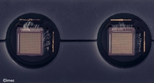
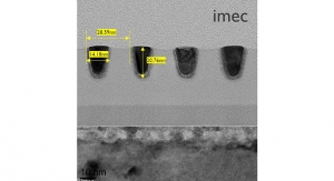
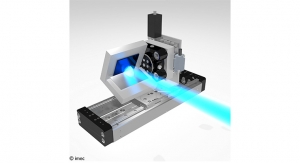
At this week’s 2017 International Electron Devices Meeting (IEDM), imec reports ultralow contact resistivity of 5x10⁻¹⁰Ωcm2 on gallium (Ga)-doped p-Germanium (Ge) source/drain contacts. The low contact resistivity and high level of Ga activation were achieved after nanosecond laser activation (NLA) at low thermal budget.
The results show that highly Ga-doped Ge-rich source/drain contacts provide a promising route for suppressing parasitic source/drain resistance in advanced pMOS devices.
These results are important in light of further downscaling of the CMOS source/drain contact area, which is challenged by a parasitic source/drain resistance and results in suboptimal transistor functioning. High dopant activation is known to be an attractive approach for lowering source/drain contact resistance.
Traditionally in pMOS devices, silicon (Si) source/drain contacts with high boron (B) activation are used. But in more advanced pMOS devices, Ge- and SiGe(Sn)-based source/drain are a promising alternative since they introduce beneficial strain.
The new findings result from a comprehensive study of Ga dopant activation in Si, Si0.4Ge0.6 and Ge conducted by imec, KU Leuven (Belgium) and Fudan University (Shangai, China).
“For the first time, we have achieved contact resistivities far below 10-9Ωcm2 for high-Ge content source/drain contacts,” said Naoto Horiguchi, distinguished member of the technical staff at imec. “This proves that Ga doping and activation by NLA or RTA are an attractive alternative to boron doping for these source/drain contacts. It provides a possible path for further performance improvement using the current source/drain schemes in next-generation technology nodes.”