11.12.18
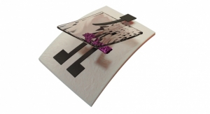
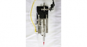
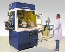
Optomec announced that the company will showcase its Aerosol Jet HD System for today’s most demanding electronics packaging challenges at the IDTechEx Printed Electronics USA show in Santa Clara, CA this week. The Aerosol Jet HD System is a compact, configurable R&D to production platform that can print a wide range of electronic materials with fine features less than 20 microns in size.
The Aerosol Jet HD System is one of a new class of micro-dispense solutions that was developed with production flexibility in mind. With its ability to print an array of electronic materials, the Aerosol Jet printer can produce high-resolution adhesive pads with features as small as 25 microns.
This supports both conductive and non-conductive attach of today’s smallest die and components, eliminating the need for manual assembly work, which increases overall throughput, eliminating wasteful end-of-line clean-up steps.
In addition to conductive materials, the system is fully capable of high-resolution printing of a wide range of common non-conductive electronics materials. Applications include MEMS bonding, seal rings, local passivation, and insulative overcoats. When coupled with conductor printing, the HD System can produce high-density cross-over and multi-layer circuitry.
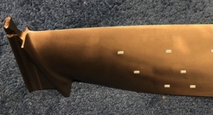
The system is capable of producing precision conformal coatings on non-planar surfaces, enabling chip and board level RFI/EMI shielding that is requisite for today’s mobile devices. Larger nozzles enable single pass printing of coatings measuring millimeters in width while maintaining uniform layer thickness from 100nm to 10s of microns. Couple this capability with Aerosol Jet’s fine feature printing and edge coatings of complex packages, selective exposure to contacts and ground planes are now possible.
The compact, modular design of the Aerosol Jet HD System enables it to easily plug into existing electronics manufacturing lines filling production gaps driven by ever decreasing product footprint challenges. The system provides a turn-key approach to advanced electronics packaging and has available production-ready recipes for a range of conductive, dielectric, adhesive and other materials, capable of extended runtimes and high yields.
At the conference, Mike O’Reilly, director of Aerosol Jet products, will deliver a presentation titled “Aerosol Jet, an Evolutionary Electronic Material Dispense Solution” in the Structural Electronics and Advanced Materials track at 5:20 pm on Nov. 14. O’Reilly will discuss how Aerosol Jet printing has been deployed for mass production/customization of sensors, antenna, and functional circuits onto non-planar substrates. He will explain how it is being used to augment wirebond applications where pad to pad spacing and multiply stacked die cause cross-talk.
Through its precise selective coating capability on all five sides of a package without depositing material on critical circuitry, Aerosol Jet printing is used as a viable alternative to PVD and Spray coating solutions. O’Reilly will explain some of the areas where Aerosol Jet printing is currently helping electronics manufacturers meet their production goals.
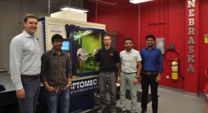
Optomec will also hold its 13th annual Aerosol Jet User Group meeting in the two days preceding the Printed Electronics USA events. The User Group meeting will be held at the Stanford University Nanofabrication facility, which houses an Aerosol Jet printer as well as other manufacturing and research equipment. User presentation topics include fully printed electronics, strain gauges, ink sintering and more. Over two dozen system owners/users will tour the Stanford lab facility and collaborate and discuss their use of Aerosol Jet printing.
The Aerosol Jet HD System is one of a new class of micro-dispense solutions that was developed with production flexibility in mind. With its ability to print an array of electronic materials, the Aerosol Jet printer can produce high-resolution adhesive pads with features as small as 25 microns.
This supports both conductive and non-conductive attach of today’s smallest die and components, eliminating the need for manual assembly work, which increases overall throughput, eliminating wasteful end-of-line clean-up steps.
In addition to conductive materials, the system is fully capable of high-resolution printing of a wide range of common non-conductive electronics materials. Applications include MEMS bonding, seal rings, local passivation, and insulative overcoats. When coupled with conductor printing, the HD System can produce high-density cross-over and multi-layer circuitry.
The system is capable of producing precision conformal coatings on non-planar surfaces, enabling chip and board level RFI/EMI shielding that is requisite for today’s mobile devices. Larger nozzles enable single pass printing of coatings measuring millimeters in width while maintaining uniform layer thickness from 100nm to 10s of microns. Couple this capability with Aerosol Jet’s fine feature printing and edge coatings of complex packages, selective exposure to contacts and ground planes are now possible.
The compact, modular design of the Aerosol Jet HD System enables it to easily plug into existing electronics manufacturing lines filling production gaps driven by ever decreasing product footprint challenges. The system provides a turn-key approach to advanced electronics packaging and has available production-ready recipes for a range of conductive, dielectric, adhesive and other materials, capable of extended runtimes and high yields.
At the conference, Mike O’Reilly, director of Aerosol Jet products, will deliver a presentation titled “Aerosol Jet, an Evolutionary Electronic Material Dispense Solution” in the Structural Electronics and Advanced Materials track at 5:20 pm on Nov. 14. O’Reilly will discuss how Aerosol Jet printing has been deployed for mass production/customization of sensors, antenna, and functional circuits onto non-planar substrates. He will explain how it is being used to augment wirebond applications where pad to pad spacing and multiply stacked die cause cross-talk.
Through its precise selective coating capability on all five sides of a package without depositing material on critical circuitry, Aerosol Jet printing is used as a viable alternative to PVD and Spray coating solutions. O’Reilly will explain some of the areas where Aerosol Jet printing is currently helping electronics manufacturers meet their production goals.
Optomec will also hold its 13th annual Aerosol Jet User Group meeting in the two days preceding the Printed Electronics USA events. The User Group meeting will be held at the Stanford University Nanofabrication facility, which houses an Aerosol Jet printer as well as other manufacturing and research equipment. User presentation topics include fully printed electronics, strain gauges, ink sintering and more. Over two dozen system owners/users will tour the Stanford lab facility and collaborate and discuss their use of Aerosol Jet printing.