09.16.19
Brewer Science, Inc. announced its participation for the 14th consecutive year in SEMICON Taiwan, which will be held Sept. 18-20, 2019, at TWTC Nangang Exhibition Center in Taipei.
In addition to showcasing its offerings in Booth N0262, Brewer Science is presenting at and sponsoring the SiP Global Summit 2019, a program on advanced packaging being held in conjunction with the conference.
Focused on “Heterogeneous Integration NOW and Future,” the SiP Global Summit will be held at CTBC Financial Park, near the exhibition center, and will span three days of presentations on various topics related to advanced packaging.
Kim Arnold, executive director, Wafer-Level Packaging for Brewer Science, will present at 2:00 p.m. on Friday, Sept. 20.
Titled “Advancement of Materials to Enable Advanced Packaging,” her talk will introduce newly developed materials and platforms for advanced packaging, especially system-in-packaging (SiP). These materials and platforms include new laser release materials, multiple-function materials, and permanent materials. She will also discuss the concept of material design and provide application examples.
Products and Technology
Brewer Science experts will be on hand in the company’s booth at SEMICON Taiwan to discuss technology trends and how Brewer Science’s products enrich people’s everyday lives, sharing details and capabilities of the products that Brewer Science will be featuring on the show floor.
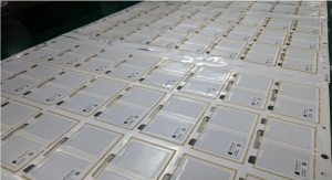
Wafer-Level Packaging
Brewer Science’s proven temporary wafer bonding (TWB) systems are designed to fit into a variety of process scenarios with minimal disruption. At SEMICON Taiwan, Brewer Science will feature its BrewerBOND dual-layer TWB system using BrewerBOND T1100- and C1300-series materials. The system is compatible with both mechanical and laser debonding methods, enables mechanical stability with no movement of bonding materials, and provides thermal stability up to 400°C. Ultrathin silicon and high-stress EMC wafers are two key applications.
Also, Brewer Science will show its BrewerBUILD multifunctional laser-assist materials, which help enable processing in wafer-level packaging. These materials offer improvements for the redistribution layer (RDL)-first build-up process, increasing both throughput and device yield and contributing to lower overall cost of ownership. Other applications include embossing, temporary bonding, laser patterning and die attach.
Lithography
Brewer Science offers products that span the entire spectrum of lithography wavelengths. At SEMICON Taiwan, Brewer Science will show its OptiStack multilayer materials and its materials for extreme ultraviolet (EUV) lithography.
OptiStack materials enable advanced multi-patterning schemes and provide room- to high- temperature stability, to keep defects low. The materials are also compatible with a broad range of lithography processes – KrF, ArF, ArFi and advanced planarization. The versatile material design allows optimization of existing multilayer processes for new nodes and products.
Brewer Science E2Stack materials are the industry standard for EUV underlayers, enabling faster development of EUV photoresist and processes. The company has also developed an innovative technique using metal-oxide-based materials to achieve higher-resolution resists and lower-dose hard masks.
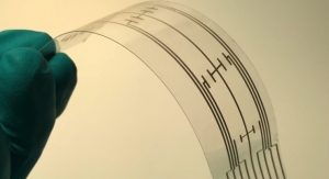
Printed Electronics
As the market for printed electronics technologies continues to grow, Brewer Science is leveraging its materials expertise in unique ways to offer complete end-to-end solutions that enrich our customers’ lives. These solutions span from printed materials to flexible electronics design, manufacturing and testing, as well as the company’s InFlect printed sensor solutions. The company utilizes unique architectures and customizable form factors to achieve near-seamless integration into existing systems for in-depth, actionable insights into processes, machinery, and the surrounding environment.
In addition to showcasing its offerings in Booth N0262, Brewer Science is presenting at and sponsoring the SiP Global Summit 2019, a program on advanced packaging being held in conjunction with the conference.
Focused on “Heterogeneous Integration NOW and Future,” the SiP Global Summit will be held at CTBC Financial Park, near the exhibition center, and will span three days of presentations on various topics related to advanced packaging.
Kim Arnold, executive director, Wafer-Level Packaging for Brewer Science, will present at 2:00 p.m. on Friday, Sept. 20.
Titled “Advancement of Materials to Enable Advanced Packaging,” her talk will introduce newly developed materials and platforms for advanced packaging, especially system-in-packaging (SiP). These materials and platforms include new laser release materials, multiple-function materials, and permanent materials. She will also discuss the concept of material design and provide application examples.
Products and Technology
Brewer Science experts will be on hand in the company’s booth at SEMICON Taiwan to discuss technology trends and how Brewer Science’s products enrich people’s everyday lives, sharing details and capabilities of the products that Brewer Science will be featuring on the show floor.
Wafer-Level Packaging
Brewer Science’s proven temporary wafer bonding (TWB) systems are designed to fit into a variety of process scenarios with minimal disruption. At SEMICON Taiwan, Brewer Science will feature its BrewerBOND dual-layer TWB system using BrewerBOND T1100- and C1300-series materials. The system is compatible with both mechanical and laser debonding methods, enables mechanical stability with no movement of bonding materials, and provides thermal stability up to 400°C. Ultrathin silicon and high-stress EMC wafers are two key applications.
Also, Brewer Science will show its BrewerBUILD multifunctional laser-assist materials, which help enable processing in wafer-level packaging. These materials offer improvements for the redistribution layer (RDL)-first build-up process, increasing both throughput and device yield and contributing to lower overall cost of ownership. Other applications include embossing, temporary bonding, laser patterning and die attach.
Lithography
Brewer Science offers products that span the entire spectrum of lithography wavelengths. At SEMICON Taiwan, Brewer Science will show its OptiStack multilayer materials and its materials for extreme ultraviolet (EUV) lithography.
OptiStack materials enable advanced multi-patterning schemes and provide room- to high- temperature stability, to keep defects low. The materials are also compatible with a broad range of lithography processes – KrF, ArF, ArFi and advanced planarization. The versatile material design allows optimization of existing multilayer processes for new nodes and products.
Brewer Science E2Stack materials are the industry standard for EUV underlayers, enabling faster development of EUV photoresist and processes. The company has also developed an innovative technique using metal-oxide-based materials to achieve higher-resolution resists and lower-dose hard masks.
Printed Electronics
As the market for printed electronics technologies continues to grow, Brewer Science is leveraging its materials expertise in unique ways to offer complete end-to-end solutions that enrich our customers’ lives. These solutions span from printed materials to flexible electronics design, manufacturing and testing, as well as the company’s InFlect printed sensor solutions. The company utilizes unique architectures and customizable form factors to achieve near-seamless integration into existing systems for in-depth, actionable insights into processes, machinery, and the surrounding environment.