12.06.19
Thin-film photovoltaic CIGS technology has seen considerable growth in manufacturing capacity in recent years.
The environmental impact, especially the CO2 footprint of CIGS thin-film panels shows great advantages compared to other solar technologies.
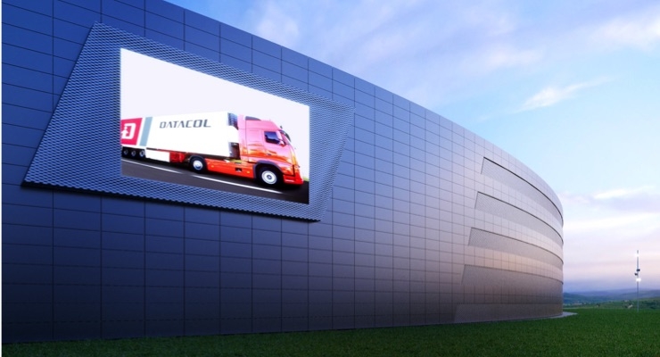
CIGS panels show good performance in diffuse light conditions and at high temperatures and are tolerant of partial shading. Additionally, the aesthetic qualities and the possibility of custom colors make CIGS a superior PV technology for the application in building-integrated photovoltaics (BIPV), e.g. in solar façades.
The fabrication process of the CIGS semiconductor layer is the key driver for both, the further increase of efficiency, and the reduction of the manufacturing cost of CIGS solar modules. Based on the European energy research program SOLAR-ERA.NET, the solar companies equipment manufacturer Smit Thermal Solutions and solar company AVANCIS started a European collaboration with the leading research institutes Helmholtz-Zentrum Berlin (HZB), CNRS (Institut des Matériaux Jean Rouxel, Nantes) and TNO/Solliance with the new project ‘Sequential, High Uniformity, Cost Competitive Elemental Selenization and Sulfurization for CIGSSe2’, called SUCCESS. The aim of SUCCESS is the combination of a further cost-optimized CIGS processing and the high efficiencies reached with heavy alkali post-deposition treatment (PDT). An efficiency of more than 20% is finally targeted for 30x30cm2 AVANCIS’ modules.
"Reaching the efficiency goal of more than 20% for a 30x30cm2 module, SUCCESS is set to pave the way for a further reduction of the total cost of electricity generated by the CIGS technology in any application from greenfield to building-integrated PV," said Dr. Jörg Palm, chief technology officer of AVANCIS.
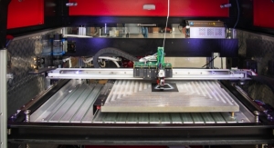
The non-vacuum Smit Thermal Solutions in-line selenization equipment provides a high degree of freedom in the CIGS semiconductor fabrication enabling further cost reduction at high-efficiency levels. Using Smit Thermal Solutions prototype pilot equipment, notable efficiencies have already been reached by TNO/Solliance and HZB at the cell level. As the first steps in scaling-up, the homogeneity of the selenization process in the Smit Thermal Solutions equipment will be improved and it will be adapted for the 30x30cm2 AVANCIS R&D platform.
During the last three years, the conversion efficiency of CIGS record cells has been increased from 20.5% to 23.35% by using controlled PDT of the absorber layer with heavy alkali metals. Typically, these records are achieved with small cells measuring 1x1cm². The consortium aims to systematically investigate the impact of the heavy alkali doping in the absorber formation process as well as by PDT of the absorber and to ultimately apply this technology to large-area module production processes with a Cd-free buffer process.
The environmental impact, especially the CO2 footprint of CIGS thin-film panels shows great advantages compared to other solar technologies.
CIGS panels show good performance in diffuse light conditions and at high temperatures and are tolerant of partial shading. Additionally, the aesthetic qualities and the possibility of custom colors make CIGS a superior PV technology for the application in building-integrated photovoltaics (BIPV), e.g. in solar façades.
The fabrication process of the CIGS semiconductor layer is the key driver for both, the further increase of efficiency, and the reduction of the manufacturing cost of CIGS solar modules. Based on the European energy research program SOLAR-ERA.NET, the solar companies equipment manufacturer Smit Thermal Solutions and solar company AVANCIS started a European collaboration with the leading research institutes Helmholtz-Zentrum Berlin (HZB), CNRS (Institut des Matériaux Jean Rouxel, Nantes) and TNO/Solliance with the new project ‘Sequential, High Uniformity, Cost Competitive Elemental Selenization and Sulfurization for CIGSSe2’, called SUCCESS. The aim of SUCCESS is the combination of a further cost-optimized CIGS processing and the high efficiencies reached with heavy alkali post-deposition treatment (PDT). An efficiency of more than 20% is finally targeted for 30x30cm2 AVANCIS’ modules.
"Reaching the efficiency goal of more than 20% for a 30x30cm2 module, SUCCESS is set to pave the way for a further reduction of the total cost of electricity generated by the CIGS technology in any application from greenfield to building-integrated PV," said Dr. Jörg Palm, chief technology officer of AVANCIS.
The non-vacuum Smit Thermal Solutions in-line selenization equipment provides a high degree of freedom in the CIGS semiconductor fabrication enabling further cost reduction at high-efficiency levels. Using Smit Thermal Solutions prototype pilot equipment, notable efficiencies have already been reached by TNO/Solliance and HZB at the cell level. As the first steps in scaling-up, the homogeneity of the selenization process in the Smit Thermal Solutions equipment will be improved and it will be adapted for the 30x30cm2 AVANCIS R&D platform.
During the last three years, the conversion efficiency of CIGS record cells has been increased from 20.5% to 23.35% by using controlled PDT of the absorber layer with heavy alkali metals. Typically, these records are achieved with small cells measuring 1x1cm². The consortium aims to systematically investigate the impact of the heavy alkali doping in the absorber formation process as well as by PDT of the absorber and to ultimately apply this technology to large-area module production processes with a Cd-free buffer process.