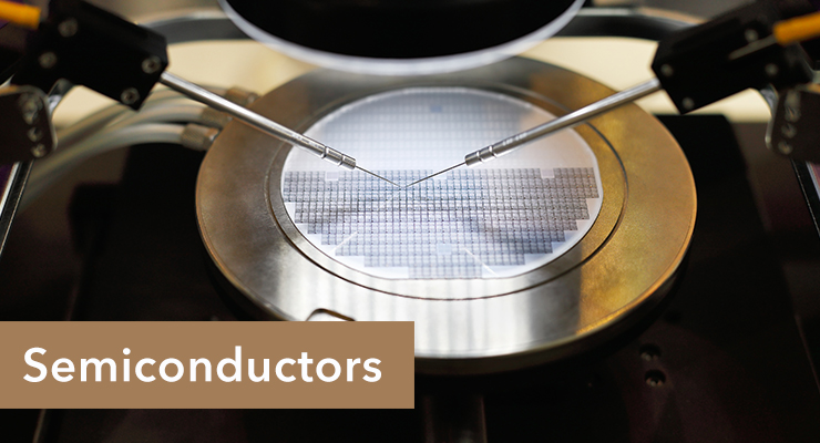
ASML, an innovation leader in the semiconductor industry that supplies chipmakers with key lithographic tools for imaging patterns on wafers, won the 2020 SEMI Americas Award.
SEMI honored the Netherlands-based firm for assembling the industry consortium that led the commercialization of Extreme Ultra-violet (EUV) lithography.
The award was presented at Virtual SEMICON West 2020.
The SEMI Americas Award recognizes technology developments with a major impact on the semiconductor industry and the world.
Efforts to extend optical lithography to wavelengths significantly shorter than ultra-violet began in the 1980s.
Since then, integrated circuit feature sizes decreased from several microns to less than 10 nanometers (nm) today, making the shift to EUV light essential.
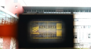
Moving to 13.5 nm wavelengths represented a paradigm shift, extending to all aspects of light generation, reflective optics, mask technologies, vacuum environment management, wafer stage alignment and a host of other fields.
ASML assembled the EUV Consortium to collaborate in meeting these challenges and developed EUV production equipment and processes. The first production system was shipped in 2013 and a total of 57 systems are currently installed in customer fabs.
“After more than 20 years of sustained R&D by ASML and its partners, EUV is now being used in high-volume chip manufacturing,” said Martin van den Brink, ASML president and chief technology officer, who accepted the award on behalf of the company. “Long-term collaboration across this technology’s value chain, from academic partners to governments and industry players, has been absolutely crucial to its success.”
ASML, founded in 1984, employs more than 25,000 people representing more than 120 nationalities in 60 worldwide locations. It has large R&D and manufacturing facilities in San Diego, San Jose, CA; and Wilton, CT.
“Outstanding engineering and industry achievements should be recognized and honored when they prompt new and emerging technologies to enhance the semiconductor industry,” said SEMI Americas president Dave Anderson. “Limitations of UV and immersion-UV lithography presented a barrier for chipmakers and halted temporarily the downsizing of microelectronics. ASML’s years-long efforts drew supply chain support as well as customer buy-in, demonstrating that the industry can tackle major problems when it comes together.”
“ASML led the effort to develop EUV lithography capability, enabling a continuation of scaling,” said Bill Bottoms, chair of the SEMI Americas Awards Advisory Committee. “The effort involved collaboration with customers and vendors and other interested parties and would not have happened without their leadership.”