Printed Electronics Now staff07.23.20
In a keynote address at the 50th annual SEMICON West, Applied Materials, Inc. president and CEO Gary Dickerson unveiled how the company is expanding the scope of its environmental, social and governance (ESG) commitments with a series of 10-year initiatives that will be driven within the company and in collaboration with suppliers, customers and the computing industry.
Furthering Applied’s new vision to “Make Possible a Better Future,” Dickerson introduced a framework for generating positive ESG impact at the company, in the industry and throughout the world.
“I strongly believe our responsibility as leaders is to leave the world in a better place,” said Dickerson. “At Applied Materials, making a positive contribution to the community is at the foundation of our culture. I am excited to join forces with our employees, suppliers, direct customers, and the computing and electronics industries to Make Possible a Better Future.”
To reduce the environmental impact of its operations, Applied is announcing the following goals: 100% renewable energy sourcing in the U.S. by 2022 and worldwide by 2030, and a 50% reduction in Scope 1 and 2 carbon emissions by 2030.
Applied also announced that it signed a power purchase agreement (PPA) with Apex Clean Energy, a key step toward reaching its renewable energy targets.
Also, the company committed to setting targets through the Science Based Targets initiative (SBTi) and reporting in line with the recommendations of the Task Force on Climate-Related Financial Disclosures (TCFD).
Applied is driving several initiatives with its customers and suppliers to promote greater sustainability industry-wide. This includes improving the eco-performance of its existing and new systems with hardware and software upgrades that reduce energy use, chemical use and cleanroom space requirements.
As part of its new “ecoUP” initiative, Applied announced a “3 by 30” goal for its manufacturing systems: on a per-wafer basis, Applied targets a 30-percent reduction in equivalent energy consumption along with a 30-percent reduction in chemical consumption, and a 30 percent increase in throughput density – which is the number of wafers processed per square foot of cleanroom space – by 2030.
Also, Applied launched the SuCCESS2030 initiative (Supply Chain Certification for Environmental and Social Sustainability) aimed at creating a more sustainable and just supply chain for semiconductor and display manufacturing. SuCCESS2030 will optimize material and parts selection, procurement, packaging, warehousing, transportation and recycling to reduce energy and emissions and conserve resources. The program also aims to promote ethics, human rights, diversity and inclusion throughout the supply chain.
“As we move from digital age to an AI age, the semiconductor industry continues to enrich lives and serve people around the world,” TSMC CEO Dr. C.C. Wei said. “At TSMC, green manufacturing is deeply embedded in our culture. Applied Materials is a key member of this initiative, and its work demonstrates how we can innovate together to reduce emissions.”
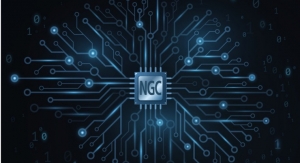
On a global scale, AI has enormous promise to accelerate research in areas such as climate change, disease prevention and public health, yet it also consumes a growing amount of power.
For AI to reach its true potential, major advances in the power, performance, area-cost and time-to-market (PPACt) of semiconductor devices are needed.
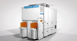
Applied is helping enable these advances with the industry’s largest and broadest portfolio of technologies and products which spans creating, shaping, modifying, analyzing and connecting structures and devices. An example of this is Applied’s new Selective Tungsten process technology that removes a critical bottleneck to continued 2D scaling in foundry-logic nodes.
“As we push deeper into the AI era, the world is growing ever more reliant on semiconductors, and our promise to create a better future for all has never been more dependent on our ability to work collectively across our industry and the electronics ecosystem,” said Dickerson. “We need to break down barriers, from Materials to Systems™ and from Systems to Materials, connecting dots in new ways between system designers, developers, integrators, chipmakers, and equipment and materials suppliers.”