02.24.21
At the 2021 SPIE Advanced Lithography Conference, imec and ASML, the world’s leading manufacturer of semiconductor lithography equipment, presented several papers that demonstrate the ultimate single-exposure patterning capability of today’s 0.33NA NXE:3400 extreme ultraviolet lithography (EUVL).
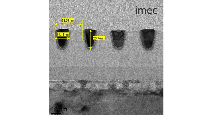
Process optimizations have enabled the patterning of dense 28nm pitch line/spaces with an Inpria metal-oxide resist in one single exposure, relevant for high-volume manufacturing.
For the first time, optical and e-beam inspections were correlated with electrical data to gain further insights in improving stochastic defectivity – i.e., both breaks and bridges.
Also, source optimizations have led to printing the smallest pitch possible with the current NXE:3400 scanner (i.e., 24nm pitch line/spaces and 28nm pitch contact holes), allowing for early material development required for high-NA EUV lithography scanners.
Extreme ultraviolet lithography has reached a critical decision point where one can move to EUV multi-patterning for printing the densest features of the next-generation ICs or push further the single print capability on today’s 0.33NA full-field scanners.
“While multi-patterning techniques would offer more relaxed pitches, single patterning enables a tremendous cost advantage and simpler process schemes," said Kurt Ronse, advanced patterning program director at imec. “Imec and ASML have demonstrated 28nm pitch single-exposure patterning readiness for line/spaces, which corresponds to critical back-end-of-line metal layers of a 5nm technology node. This brings the NXE:3400 scanner very close to its resolution limit for high-volume manufacturing.”
The results were obtained using Inpria’s metal-oxide (MOx) resist process.
To increase learnings on stochastic patterning failures, defectivity inspection data obtained with scanning electron microscopy, broadband plasma and e-beam technologies were successfully correlated with data obtained from electrical measurements.
The electrical tests were carried out on large-area ruthenium-metalized serpentine structures that allowed to measure electrical opens (and hence bridges in the resist), as well as on metalized fork-fork and tip-to-tip structures that allowed to measure electrical shorts (and hence critical breaks in the resist).
Besides showing a good correlation, the complementary electrical measurements allow capturing important trends across multiple process changes that can help to mitigate stochastic printing failures (papers n° 11609-26; 11611-21).
The extendibility of 0.33NA EUV lithography to pitch 28nm resulted from co-optimizing the various contributors to the patterning process, including mask templates, illumination settings, metal-oxide resist and etch processes.
For example, the benefits of using bright-field mask tonality and controlled lens aberrations were shown to largely improve the printability at a small pitch and critical dimensions (papers n° 11609-27; 11609-29).
Besides pushing the boundaries of single-exposure EUVL for high-volume manufacturing, imec and ASML have brought the 0.33NA NXE:3400 to its extreme resolution to use it as a platform for early material development for the high-NA EUVL tools.
“Imec and ASML recently also showed the tool’s capability of printing 24nm pitch line/spaces and 28nm pitch contact holes – the latter by optimizing pupil and imaging conditions and by using double line/space exposures at a combined dose of 45mJ/cm2," said Steven Scheer, VP advanced patterning process and materials at imec.
“Pattern transfer could be successfully demonstrated on very thin resists that are relevant for high-NA EUV," saidAndrew Grenville, CEO of Inpria. “This will provide the imec patterning ecosystem with the opportunity to develop resist, metrology and etch processes to accelerate the introduction of the next-generation EUVL system, i.e., the high-NA EXE:5000.”
Added Scheer: “These developments will complement the learnings that are currently being obtained from imec’s attosecond analytical and interference lithography lab (the AttoLab), expected to offer a high-NA resist imaging capability to print features down to pitches as small as 8nm.”