02.28.23
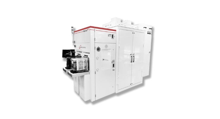
Infinitesima has completed the first customer shipment of the Metron3D metrology system, a sub-nanometer, high speed 3D imaging system that operates at in-line production throughputs. The system has passed all internal qualification tests for imaging quality and throughput and is being shipped to an undisclosed, leading semiconductor manufacturer.
With imaging time measured in seconds, rather than minutes the system will address metrology challenges for manufacturing next generation logic, DRAM and 3D NAND devices.
The company reports that the Metron3D has demonstrated throughput and imaging speeds up to 100x faster than conventional atomic force microscopy (AFM) technology, achieved through a patented photo-thermal actuation of the probe tip. To ensure imaging quality in a manufacturing fab environment, the system has been designed to withstand acoustic noise and vibration through resonance modelling and multi-layer acoustic isola-tion.
Technology inflections towards High NA EUV, hybrid wafer bonding, and complex 3D de-vice structures are now moving beyond the capability of existing e-beam and optical tech-niques and are a limiting factor for further progress.
A key example is the coming transition to High-NA EUV, where smaller features require higher resolution metrology, but the thinner resists reduce image contrast and are more sensitive to damage when using e-beam techniques. Probe metrology is well established as a lab technique and has the resolution and 3D imaging capability to overcome these challenges but has traditionally been too slow for in-line integration. The Metron3D breaks this paradigm, providing probe metrology at the high throughput necessary for in-line process control.
