04.24.24
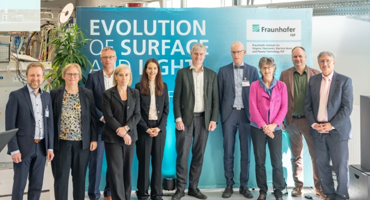
The Fraunhofer Institute for Electron Beam and Plasma Technology FEP expands its campus with the RESource-Efficient Energy Technologies (RESET) research center in Dresden. With state-of-the-art laboratory facilities for sputter epitaxy, biomedical applications and electron beam technologies, the institute aims to set new standards in research.
The strategic research focus for activities in the building are the development of innovative process technologies, for example for the generation, storage and processing of hydrogen (power-to-X) and for the deposition of high-precision gallium nitride (GaN) layers on silicon wafers.
As one of the first Fraunhofer Institutes in Dresden, the Fraunhofer Institute for Electron Beam and Plasma Technology FEP has been a fixture in the research landscape of the Saxon state capital for more than 30 years.
The institute applies its specialized core competencies in electron beam and plasma technology to develop innovative surface functionalization processes and vacuum technologies for a wide range of substrates, from flexible films and bulk materials to metal strips and ultra-thin glass.
In addition to coating and process development for customers and partners from a wide range of industries, the Fraunhofer FEP is able to offer these processes in-house, from laboratory tests to pilot production.
This provides customers with a reliable basis for transferring complete processes for surface modification and thin film coating to commercial application based on the institute’s access to plant technology infrastructure ranging from laboratory scale to industrial sheet-to-sheet and roll-to-roll coating lines and systems for precision coating.
“I am happy and proud to see that the campus is expanding to include state-of-the-art laboratories for biomedical applications, a clean room for our research in the field of sputter epitaxy, as well as its attractive rooms for creative and collaborative work for our researchers,” Institute director Prof. Elizabeth von Hauff said.
The planned research projects at RESET are determined by the establishment of a globally unique electron beam competence and technology center. The completed building ensemble now houses facilities for the development of non-thermal electron beam technologies for medical, biotechnology, environmental and energy applications.
In addition, a clean room has been set up for research into highly innovative process technologies for sputter epitaxy. A Fraunhofer FEP research group is dedicated to the development of magnetrons and process technologies for sputtering thin layers, e. g. gallium nitride (GaN) layers, on 200 mm silicon wafers and obtaining epitaxial layers.
The resulting GaN semiconductors with high-precision layers are to be used in future in power electronics or in applications such as light-emitting diodes (LEDs). In the course of the year, the research group will have a new wafer-based high-temperature and ultra-high-vacuum PVD system available for this purpose, equipped for the first time with wafer handling in accordance with ISO3.