04.25.24
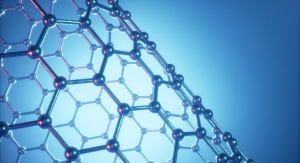
Multi project wafer (MPW) runs are a common practice within the semiconductor ecosystem. Universities, R&D centers and start-ups, which usually only need a few prototypes and operate with tight budgets, take advantage of this service to obtain devices at an affordable entry point.
This is carried out with a mask sharing scheme, where devices with different geometries but shared device architecture are manufactured within the same mask; in this way, everyone gets a few devices but no one needs to purchase more devices than necessary.
Now, Graphenea partners with the 2D Experimental Pilot Line (2D-EPL) to offer an MPW run with a novel process flow. Operating within the 2D-EPL under the auspices of the Graphene Flagship, Graphenea Semiconductor unveils a cutting-edge process flow that aims to redefine possibilities in device architecture and application versatility.
At the heart of this innovation lies a novel device fabrication process flow crafted by Graphenea. This framework unlocks the potential for three distinct device architectures, catering to a spectrum of applications spanning from general electronics to advanced sensing and optoelectronics. Central to this advancement is the utilization of HfOx as the dielectric material. Complementing this, the introduction of AlOx as the passivation layer adds further resilience
Despite its experimental nature within the 2D EPL, Graphenea brings to the table a wealth of experience in fabricating Graphene Field-Effect Transistors (GFETs), having successfully manufactured over half a million units.