04.26.24
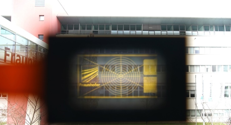
As part of the HOT project (High-performance transparent and flexible microelectronics for photonic and optical applications), scientists from the Fraunhofer Institute for Photonic Microsystems IPMS have developed a semi-transparent microdisplay.
This microdisplay is significantly lighter than conventional combiner-based optical see-through near-to-eye systems and offers high resolution. The microdisplay will be presented at the SID Display Week 2024 in San Jose, USA, at the German Pavilion, booth number 1124.
In today's time, more augmented-reality (AR) glasses and see-through systems with different application areas are entering the market. To increase the acceptance of these devices and improve wearing comfort, it is important that they are lightweight and easy to use.
For mobile consumer electronics devices, the key acceptance criteria are form factor or compactness (volume, weight), battery life, connectivity, app ecosystem, and cost.
OLED microdisplays are ideal as image generators for virtual-reality (VR), augmented-reality (AR), and mixed-reality (MR) applications, due to their high resolution and technological level/maturity. However, these microdisplays are typically not transparent due to their silicon-based technology.
Therefore, a complex optical system is required for use in see-through data glasses and similar devices, which allows the combination of real and virtual images (optical combiner). This has significant implications on the weight, size, and optical efficiency of the entire glasses.
The scientists at the Fraunhofer Institute for Photonic Microsystems IPMS’ newly developed semi-transparent OLED-on-silicon microdisplay technology opens new possibilities for optical design of slim, near-eye optics. Depending on the design approach, microoptics can already be directly integrated on the chip.
"Modern and advanced silicon CMOS processes are increasingly being applied to silicon-on-insulator (SOI) wafers,” said Philipp Wartenberg, group manager IC and System Design at Fraunhofer IPMS. “This wafer technology can be used for implementation of very thin circuitry layers. With the help of a specific IC design and an appropriate process flow which enables transfer on a glass wafer semi-transparent microdisplays are possible."