David Savastano, Editor05.22.13
The organic light-emitting diodes (OLEDs) and organic photovoltaic (OPV) fields remain a very interesting opportunity for functional materials manufacturers. If materials suppliers can solve certain technical challenges, the field could open up.
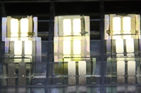
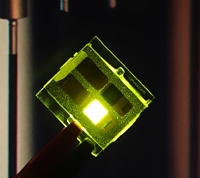
cynora GmbH is close to commercializing these materials. A growing company located in the high-tech incubator at the northern campus of the Institute of Technology in Karlsruhe (KIT), cynora specializes in the research and development of innovative copper-based functional organic semiconductor materials for OLEDs. Copper is an ideal material, as it is favorably priced and readily available. cynora believes this will allow OLEDs to be printed as foils just like newspapers, using inkjet or slot-die-coating.
cynora’s materials can be used to print light onto thin foils, labels or as part of smart packaging. The application of these materials is also possible in lasers, printed organic sensors or bio-labels in cell studies.
cynora is on the verge of entering the market this year, based on evaluation agreements with pilot customers. Since 2008, the company has been steadily working on increasing its position for market-entry by enhancing its IP portfolio, and the company’s leaders report that cynora’s most recent cyEmitters show impressive performance in preliminary tests.
“Now we are establishing an OLED device setup that will take advantage of this potential,” said Dr. Tobias Grab, CEO of cynora. “Our optoelectronic solutions combining new material structures with the capability for solution-processing have attracted much interest, which is why we are confident that we are on the right way.”
Dr. Grab noted that the most important markets for OLED technology are expected to be display and lighting.
“Since current process technology has limitations in terms of substrate sizes, we believe that solution-based processes are the best choice for large-area OLEDs, which enable new lighting forms,” he said. “Consequently, cynora’s proprietary technology for crosslinking of solution-processed layers in order to enhance the stability is an important step towards printed white light.”
It is no surprise that there are challenges with developing functional materials; Dr. Grab noted that cynora has overcome some of these concerns.
“Early obstacles such as problems caused by interactions with water or air have been solved by careful analysis and material design,” Dr. Grab said. “The processing of the materials, however, is currently a technical challenge. The multilayer structure of the devices can change during operation, resulting in partial mixing of the layers and a reduced device performance. Avoiding this mixing is especially relevant for solution-processed devices, since it can also be caused by the wet deposition process itself.
“With this in mind, the goal of cynora is to provide concepts for OLEDs from solution,” Dr. Grab added. “This involves a patented modular emitter system with controllable solubility of the materials as well as a stabilization of the layers in order to prevent mixing during production and device operation. Both aspects have been combined in cynora’s innovative crosslinkable inks, which become insoluble after deposition, enabling us to produce stable multilayer architectures from solution.”
Dr. Grab said that the next step for cynora involves material testing by interested device manufacturers, and the company is working on partnerships with OLED manufacturers.
“Cooperations with panel producers are the most efficient way to improve or adapt the material portfolio or to expand existing materials,” Dr. Grab said. “After successful implementation of our materials into processes with leading players in the OLED manufacturing industry, the next long-term opportunity will be the completion of licensing agreements for long-term commitments.
“Since the OLED market is still at a relatively early stage, the printed OLED market in particular, our aim is to open the market in 2013 and actively shape it in the following years,” Dr. Grab concluded.