David Savastano, Editor03.25.14
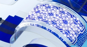
Due to their unique nature, flexible and printed electronics have a wide range of needs. Equipment manufacturers are developing new machinery that are helping printed electronics systems begin to reach their potential.
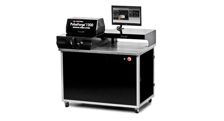
Stan Farnsworth, vice president of marketing for NovaCentrix, said that NovaCentrix recently released the PulseForge 1300, an R&D platform based on the power of the company’s PulseForge 3300 tools but in the chassis of its PulseForge 1200 tools
“The PulseForge 1300 is able to process the semiconductor materials and TCO materials that are of such interest in the market right now,” Farnsworth said. “Process conditions that are developed on the PulseForge 1300 can then be immediately applied in production on the full-size PulseForge 3300 tools. We have also recently updated the software engine that drives our SimPulse simulation, which is an important tool for designing the material stacks and with the exact same user interface as our actual PulseForge tools. Look for increased accessibility to the SimPulse application very soon.”
Xenon Corporation CEO Lou Panico said that as a manufacturer of high energy pulsed light systems, XENON is continually developing systems that offer increase performance, power and flexibility.
“This is particularly true for the printed electronics industry, where low temperature sintering of conductive inks creates unique challenges for photonic sintering,” Panico said. “One aspect of this challenge is the deep sintering of thick conductive inks, where the demand is not only higher energies but also methods of managing the thermal properties of optical energy delivery over time, to allow sintering action to take place through the thick conductive layer yet not elevate the substrate temperature significantly.
“To overcome the penetration of cure issue, XENON has developed a dual pulse mode system where a single pulse comprising of two superimposed pulse profiles,” Panico added. “These two independently controllable profiles, allows the first pulse to bring the ink into the sintering active region. The second profile can be adjusted to maintain the thermal characteristics for a longer period of time for improved sintering. Early testing of this process suggest that a better than 50% improvement of the resistivity can be achieved in the sintering of silver and copper inks.”
Thomas Kolbusch, vice president, Coatema Coating Machinery GmbH, reported that Coatema has launched a large number of innovations.
“We introduced the Thinfilm Coater/Printer to the market, a high tech S2S tool for precise printing and coating of complete devices,” Kolbusch said. “The BC 3G a big scale pilot coater to perform inline production processes up to 800 mm working width. The Smartcoater is now available to integrate inkjet, laser and UV nano imprint. And if everything works out, we will show a new product range at LOPEC 2014.”
David Ventola, director business development – Advanced Materials processing at MEGTEC Systems, Inc., noted that MEGTEC’s history is large industrial equipment, and added that in the current state of the PE market, there is a need to support the R&D of new products.
“To meet the needs for R&D organizations, we launched a lab scale machine with standard features and the flexibility to customize for a given application,” Ventola said.
Nicolas Bernardin, deputy managing director and oo-founder of Ceradrop, said that Ceradrop MGI Group’s most recent innovative inkjet deposition products is the X-series stand-alone system, which exclusively offers CAD/CAM solutions for printed electronics developments.
“The X-series has fully integrated UV, IR, adphosNIR and PulseForge post solutions printed curing requirements and options,” said Bernardin. “It has up to three printheads for three materials solutions processing, while allowing for automatic printed switching for ease of integration and process developments from a stand alone system solution.”
Bob Hoffman, regional manager, Martin Automatic Inc., said that customers are coming to Martin for its expertise in how to transport a web from point A to point B.
“On the one hand, our customers are running materials that are getting ever thinner and more delicate – films such as 0.0005 in (12 micron) polyethylene and 0.00025 in (6 micron) PET, and materials like 0.00025 in (6 micron) “dead soft” (or 0-temper) aluminum foil – and we’re designing and building automatic roll changers to meet processing speeds to 914 M/min,” Hoffman said.
“As one example, Martin has developed the advanced Airnertia roller technology that offers lowest roller inertia and essentially friction-free rotation,” Hoffman added. “Airnertia is one of Martin’s many technology applications for splicing and transport of lightweight and delicate web materials. On the other end of the spectrum, we have customers who run some incredibly expensive materials at very slow speeds, but they can’t afford tension upsets or stoppages for roll changes. And Martin’s expertise extends both to narrow roll applications and those as wide as 160 in (4 m).”
Jürgen Kreis, director business development, AIXTRON SE, said that AIXTRON continues to further improve its proprietary OVPD and PVPD technologies to enable customers to address an even wider range of commercially viable applications.
“As one example, we have designed and optimized our STExS source technology as one fundamental building block of our OVPD process technology,” Kreis said. “The latest improvements allow for enhanced throughput by enabling high deposition rates while at the same time lowering the thermal stress of the sensitive organic materials. With the development of the large area demonstrator (please see q.3) we enhance our showerhead technology to allow free scalability to industrially relevant sizes, to enable economic organic layer deposition up to a substrate size of Gen8 (2.300 mm x 2.500 mm).”