David Savastano, Editor02.03.16
The market for flexible and printed electronics is growing, and in many cases, these products came out of projects at the university level. In speaking with academic leaders, there are new projects coming out of colleges and universities that are showing potential.
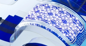
“There are two very interesting projects worth mentioning here: OLED-3D and FIM-O,” said Prof. Klaus Meerholz, Department Chemie, Universität zu Köln, and the COPT.CENTRE. “Both resulted in the realization of impressive demonstrators (photo OLED-3D) that attracted a lot of attraction in industry and press. In OLED-3D, a new method to produce OLEDs on 3-dimensional substrates by very simple solution-processing was developed and demonstrated. With automotive being one of the most attractive application sector for such OLEDs, the projects consortium consisted of Audi, Automotive Lighting, Philips, Merck and the University of Cologne.
“FIM-O used Film-Insert-Moulding to integrate organic electronics into 3D-shaped free form plastic housing to create high quality mountings,” Dr. Meerholz added. “Those mounting were realized within the projects with integrated solar cells and OLED display function in various colors by the project partners Bö-La Siebdrucktechnik, Konststoffinstitut Lüdenscheid, ZOEK GmbH and University of Cologne. The big markets for such mountings are two-fold: automotive (black housing) and domestic applications (white housing).To realize high performing OLEDs, it is crucial to stack different organic materials with different functions.”
Using solution-based, e.g. printing, methods, this is not trivial, since dissolving can occur. “In Cologne, crosslinkable materials that can be made insoluble after deposition have a long tradition,” said Dr. Anne Köhnen, scientific manager of the COPT.CENTRE in November. “Those materials are the basis for most of our projects and will be also in future, to bring printed electronics to a high level performance.”
Prof. Shlomo Magdassi, The Enrique Berman Chair, Casali Center, Institute of Chemistry, The Hebrew University of Jerusalem, said that in the field of printed electronics, he and his team are working on a variety of interesting projects.
“Two of the most advanced were already licensed to companies: Nano Dimension, making 3D printed circuit boards, and ClearJet, printing transparent touch screens for smartphones, etc.,” Prof. Magdassi said. “We are currently involved in additional exciting projects - to name a few: printing actuators for soft robotics, 3D printing of conductors and shape memory materials, printing large format light detectors, synthesis of low cost conductive copper inks.”
Bernard Kippelen, director, Georgia Tech - Center for Organic Photonics and Electronics (COPE), said that with more than 30 faculty members working on various aspects of organic photonics and electronics, pointing to a single project is difficult.
“The spectrum of really interesting projects spans from advances in materials (e.g. development of new organic electric dopants to produce n-doped semiconductors), to the fabrication of supercapacitors with unprecedented energy storage density of 40 J cm-3 (Advanced Energy Materials, DOI: 10.1002/aenm.201500767) to the first demonstration of a carbon nanotube optical rectenna device (Nature Nanotechnology DOI: 10.1038/NNANO.2015.220), a device that directly converts electromagnetic waves a optical frequencies into dc currents, to the demonstration of organic-light-emitting diodes on shape-memory polymers, materials that are rigid at room temperature but become soft at temperatures of the human body (Organic Electronics, DOI: 10.1016/j.orgel.2015.06.029),” added Kippelen.
Dr. Bruce E. Kahn, adjunct professor of graphic communications, The Sonoco Institute of Packaging Design and Graphics at Clemson University, said tha Clemson is currently completing a project on ambient RF energy harvesting using printed metamaterials.
“This project is very exciting and extremely timely,” Dr. Kahn said. “Although some types of energy harvesting (e.g. solar, wind, thermal) are very popular and have been well studied, they all have limitations. For example, solar power only works when there is light (during the day time), and can be limited by factors such as weather. RF energy has a number of potential advantages. It is available at all hours, can be transmitted through walls, and many of the devices that we commonly use are already set up to receive it. Given the proliferation and growth of wireless devices, the amount of available RF energy in the environment will continue to increase for the foreseeable future.
“At the same time, electronic devices continue to become increasingly power efficient (a consequence of Moore’s law). Together, these factors show that the case for RF energy harvesting gets better every day,” Dr. Kahn added. “However there are a number of challenges that must be addressed before RF energy harvesting can be widely utilized. Fortunately, many of these challenges can be addressed using flexible hybrid electronics. We are currently printing metamaterial inspired antennas, which collect RF energy very efficiently, compactly, and over a wide range of frequencies. The ability to print flexible, large area antennas and arrays will help enable the collection of more RF energy. Our RF energy harvesting designs are hybrid systems in that they use silicon components to convert the collected RF energy into useful power. The silicon components are attached to the printed antennas. These energy harvesting systems should be able to provide power over long periods of time to charge batteries, and enable new types of wearable and embedded devices.”
“We are currently working on capacitive sensors for a variety of applications, beyond touch sensors,” Dr. Malcolm G. Keif, professor and graduate coordinator, Printed Electronics & Functional Imaging for the Cal Poly State University’s Graphic Communication Department, noted. “Also, applications for consumer packaging remain of interest.”
Dr. Takao Someya, Department of Electrical and Electronic Engineering, School of Engineering, the University of Tokyo, reported the university is developing ultraflexible and strethcable sensors that can detect vital information without causing discomfort of wearing.
Dr. Patrick J. Smith, Department of Mechanical Engineering, University of Sheffield, pointed to in-situ formation of PANI/Ag using reactive inkjet printing as a project of note.
“Stretchable electronics that are biocompatible has been one of the more interesting projects we have worked on,” Dr. Margaret Joyce, professor in the Department of Chemical and Paper Engineering at Western Michigan University and director of WMU’s Center for the Advancement of Printed Electronics (CAPE), said.
Eric S. Howard, corporate and outreach manager, NSF Center for High-rate Nanomanufacturing at Northeastern University, noted that some of Northeastern’s most interesting projects are still covered by non-disclosure agreements.
“During the last six years, we’ve filed about 55 patents, and 14 have been awarded, so some of them are now in the public domain.,” Howard added. “We are particularly excited about incorporating nano-scale particles into biosensors. When the target molecule comes in contact with the sensor, that creates a change in the sensor’s electrical conductivity, creating a signal that we can measure. We have been testing this sensor platform on cancer biomarkers as well as biomarkers for fatigue and over-exertion, and the preliminary results show it to be 100-1,000 times more sensitive than commercially-available ELISA-type tests. Enzyme-linked immunosorbent assay (ELISA) is a test that uses antibodies and color change to identify a substance, while we use the electrical signal.”
“We have a lot of interesting projects but if I had to pick one that typifies the value of PERC it would be our work on the fabrication of Low-Cost Phased Antenna Arrays by 3D Printing,” said Craig Armiento, director of the Printed Electronics Research Collaborative (PERC) and co-director of the Raytheon-UMass Lowell Research Institute (RURI) at the University of Massachusetts Lowell. “This government-funded project was a Phase I STTR with two PERC members - SI2 Technologies and Raytheon. The combination of the three PERC members provided the broad range of expertise (from system integration to material development) required for the project. We were able to use 3D printing to create a dense array of Vivaldi antennas. These arrays typically use individual antennas that are hand assembled into arrays that require a level of precision similar to a Swiss watch. The effort also showed the feasibility of incorporating semiconductor ICs into the printed structure. The Phase I effort proved the feasibility of our printed approach and the promise of much lower cost arrays. We have submitted a proposal for Phase II funding to refine the work towards a fully-functional array.”
“In the early days of nanotechnology we worked on the simplest, and also printable, architecture: a network of nanoscale wires, a Nanonet if you wish,” said George Gruner, distinguished professor, Department of Physics and Astronomy, University of California Los Angeles.”Depending on the wire – carbon nanotube, silver nanowire and the like - one can make semiconducting, and metallic films, electrically conducting films that are transparent to visible light, films that can serve as the conducting channels is transistors. One can also regard these Nanonets as platforms or scaffolds. One can make composites – say carbon-oxide composites - and these can be tailor-made for energy storage, of electrodes for catalysis. One can combine scaffolds with molecules such as porphyrine, a molecule in leafs to make a photosensor, combine these with recognition biomolecules for electrical and electrochemical biosensors.
“Most of the activity in the area of printed electronics is not on polymers, but materials in the micro or nano-scale, that can be embedded in a slurry and printed,” Gruner added. “A number of research and R&D groups are conducting research on the various elements of the printed electronics landscape at UCLA. Several research groups focus on new materials, or ‘old’ materials in new shapes and forms such as graphene and other 2D materials like nanosheets, nano-scale materials as examples, with carbon nanotubes still in play. There is a general expectation that nanomaterials will be and important component of the printed electronics landscape.”