Sean Milmo, European Editor07.02.18
The European printed electronics sector has now reached a crucial point in its short history where it needs to focus much more on speeding up the commercialisation of its research discoveries.
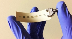
Only relatively few companies in the sector have successfully commercialized technologies. But in the short-to-medium term, it looks increasingly likely they will be joined by many others because of the relatively large number of products now being taken from the prototype through to the market launches stage, particularly using low-cost large area electronics (LAE) technologies.
“A new paradigm in large-area manufacturing is here with up to 100 times lower capex per front-end die than traditional lithographic bulk-silicon processing,” Davor Sutija, chief executive of Norway-based Thin Film Electronics ASA, a global leader in near field communication (NFC) with printed electronic smart packaging, told a recent LAE conference in Cambridge, England.
He was referring to the planned scaling-up this year of Thinfilm’s former Qualcomm-owned plant in San Jose, CA, to an annual output of 7 billion NFC tags applying technologies like rapid thermal processing instead of traditional annealing and components and circuits containing thousands of transistors made through roll-compatible manufacturing steps.
The speeding-up of technologies to industrial-scale production was a major theme of the conference organised by the Cambridge University-based Centre for Innovative Manufacturing in LAE (innoLAE) at the state-funded Engineering and Physical Sciences Research Council (EPSRC).
Commercialisation has to be achieved with low-cost processes without undermining product standards such as consistency, reproducibility, flexibility of materials, high resolution, conductivity and durability, the conference was told.
Developers have also to resolve issues like how much they should rely on predominantly organic or hybrid materials to meet the increasing demands of end-users.
Often, in order to accelerate the scaling-up process, the priority is to have the freedom to use existing organic- and hybrid-based materials and processes to cut development costs by eliminating the need for extra capital expenditure on new machinery.
One means of both reducing later stage R&D costs and speeding up commercialization is for developers to form partnerships with end-users, particularly those already well established in industrial scale production. There is a growing trend for European innovators to link up with Asian, especially Chinese, electronics producers.
FlexEnable, Cambridge, England, last year reached a licensing deal with Truly Semiconductors, one of China’s largest display makers, on the UK company’s organic liquid crystal display (OLCD) technology. Truly, which is the first display maker to adopt OLCD, is expected to start mass production in China later this year.
“This low cost process has been demonstrated on commodity plastics, which have been integrated into highly functional plastic LCD modules,” Francesca Bottachi, yield engineer at FlexEnable, told the meeting. “The process has been designed so that it can be easily transferred into existing display factories, proving a quick route to high production capacity and yields,”
In January this year, NeuDrive Ltd, a UK-based developer of organic semiconductor formulations for making rollable or foldable portable display devices with robust organic thin-film transistor (OTFT) backplanes, agreed to set up a joint venture in China with Cocoon Corp, a Chinese technology incubator organization. The venture’s first OTFT pilot line will be built in Xianning with the help of city government funds.
A low temperature process for OTFT production developed by NeuDrive enables a wide range of plastic substrates types and thicknesses to be used for dynamically flexible displays, Simon Ogier, the company’s chief technology officer, said at the conference.
Within the UK itself, EPSRC has helped form a supply chain collaboration for the development of laser induced forward transfer (LIFT) technology for digital processing of printed electronics by transferring material via short pulse laser from a donor to a receiving substrate. It has involved Swansea University’s Welsh Centre for Printing and Coating, laser specialists Oxford Lasers Ltd and industrial end-users including NeuDrive and Cambridge-based PragmatIC, a global leader in ultra low-cost flexible integrated circuits.
The group investigated the optimizing parameters for single-micron LIFT technology in order to achieve high resolution features on the acceptor substrate. Swansea University’s Davide Deganello described how the project assessed different thin film depositions by analyzing uniformity, ink rheology and optical transmission.
Among other recent advances in materials, particularly nanomaterials, and in printing processes aimed at shortening the period between prototyping, demonstration and market launch was extended applications of Nano Imprint Lithography (NIL)
Thomas Kolbusch, vice president, Coatema Coating Machinery GmbH, a German specialist in coating, printing and laminating processes and equipment, told the meeting his company has been using NIL for creating with R2R systems surface structures on polymer film, stainless steel and flexible glass.
NIL can have the disadvantage of inadequate resolution and low throughput, he said. With an R2R UV system, based on seamless sleeves on a roller, nanostructures can be transferred to the UV lacquer on the surface of polymer and other flexible substrates.
“We get a much higher throughput and resolution with the UV NIL as well as a quicker printing process with better uniformity,” said Kolbusch.
Chris Evans, a materials development scientist at UK-based Peratech Holdco Ltd., said that his company had been developing quantum tunnelling composite (QTC) inks which are compatible with flexible printed circuit sets. This is enabling force-sensing components to be applied to a wide range of electronic products.
Peratech, which hold intellectual property rights to QTC formulations and manufacturing processes, has been shaping nanoparticles in composite inks to enhance the conductivity of touch sensors. The inks can be tailored to suit specific component applications in printed circuits.
Finding ways to accelerate commercialization does not solve all the key problems arising in the later stages of development of electronics innovations. Forming partnerships with companies with production capacity and with businesses able to help with marketing still remain a major challenge for developers. But it should help to sort out difficulties like, for example, late stage funding and finding customers because of the ability to demonstrate products through the supply of samples. Above all, it will help to quickly boost the overall size of the printable, flexible electronics market.