Anthony Locicero, David Savastano, Associate Editor with Editor10.17.18
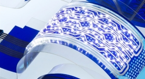
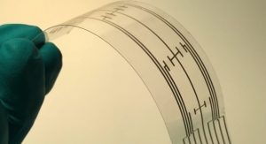
Electronic and conductive inks are a critical element in the fast-growing field of flexible and printed electronics. Estimated at $2.5 billion in annual sales, electronic and conductive inks and materials are found in a wide range of applications, from photovoltaics and flexible displays to sensors, wearables and smart packaging.
The latest conductive ink technologies, as well as key end markets, were highlighted during the inaugural Electronic and Conductive Ink Conference, which was held Oct. 11-12 at Pheasant Run Resort in St. Charles, IL, near Chicago. The conference was sponsored by the National Association of Printing Ink Manufacturers (NAPIM), Ink World and Printed Electronics Now, and was held in conjunction with NAPIM’s annual NPIRI Technical Conference. In addition, the conference featured informative tabletop exhibits as well.
With an eye on this growing market, the Printed Electronics Now’s inaugural Electronic and Conductive Inks Conference featured industry experts discussing the future of conductive ink and its role within the printed electronics spectrum. The conference opened up with Dave Savastano, editor of Ink World and Printed Electronics Now, who covered “Conductive and Electronic Inks.”
Savastano discussed some of the initial successes in the printed electronics market, including glucose test strips and RFID, as well as a few of the missteps, including organic photovoltaics. The advent of flexible hybrid electronics, merging silicon and printed technologies, is opening many new opportunities and commercial successes, including smart packaging, wearables and sensors, in-mold electronics and much more. Ultimately, conductive inks will play a major role here.
“The future of conductive inks is clearly intertwined with that of flexible and printed electronics,” Savastano concluded. “As these systems make their way into our everyday lives, the inks needed to make these systems function will continue to grow in usage. The Internet of Things, which could potentially require billions and even trillions of sensors, will change the way we live.”
Dr. Ajay Virkar, co-founder and CTO of C3Nano, followed with a look at “Activegrid™: A Flexible Transparent Conductor with Outstanding Optoelectronic Properties.” Dr. Virkar noted that C3Nano was founded in 2010 out of Stanford University, and the company has raised $40 million in investments to date, including financial support and partnerships with NISSHA and Hitachi Chemical.
The company is focused on consumer electronics and created an alternative to indium tin oxide (ITO) called Activegrid. “It’s inherently flexible,” Dr. Virkar said of C3Nano’s product. “You can’t flex an ITO without it cracking.”
With transparent conductor technology, manufacturers must decide between using carbon-based materials or metal on touch panels. While metal mesh has very high conductivity, it “gets very low resistances,” Dr. Virkar noted. “It’s less flexible.”
Silver nanowires can be a direct ITO replacement. The use of silver nanowires – long filaments of silver – dates back to the 1990s. The “millions of metal sticks” are highly conductive, offering very high transmissions, Virkar said.
However, it can cause haziness. Conductive polymers are another direct ITO replacement and offer low reflectivity while being flexible. The conductivity is much lower, however.
“The primary issues preventing the widespread adoption of non-ITO alternative methods are optics and reliability,” Dr. Virkar explained. By adding silver nitrates, manufacturers can produce very thin wires for better optics. There is more absorbance, according to Dr. Virkar, and it is less visible. C3Nano created Nanoglue, which fuses nanowires chemically, he said. Nanowires are coated with noble metals – platinum and silver – creating a less reflective surface.
The company also produces a line of inks under the name Onyx. According to Dr. Virkar, the inks eliminate reflectivity, and in some cases, it makes a screen so dark it appears the device is turned off.
In the near future, Dr. Virkar said he expects to see “small scale” flexible electronic products in the market.
Liam O’Hara, associate professor, Department of Graphic Communications, Clemson University, prepared the next talk, “Printed Electronics and Functional Printing: Research at Clemson.” Sadly, O’Hara had a family emergency, and Savastano stepped in to give the presentation.
O’Hara’s students use an Omet Varyflex 530 to conduct printed electronics studies. The modular press is configured for flexo, but a rotary screen and gravure deck have been added. Graphic inks are engineered for color, slip, rub-resistance, drying speed, adhesion, odor, gloss, chemical resistance, flexibility, temperature range, and on and on and on.
Printed electronics inks are engineered for various functionalities as well, but the industry is in its infancy and there is a tremendous need for improvement. Resolution is one challenge that needs to be worked on, as finer features enhance device performance. While printing offers high throughput, it can’t match the resolution and performance of traditional, subtractive fabrication. There’s generally an inverse relationship – high-resolution processes are low throughput; print is high throughput with low resolution.
George Fuchs, NAPIM’s director of regulatory affairs and technology, closed the morning session with “Managing Health and Safety Issues Associated with Engineered Nanomaterials.
“Our current understanding of health, safety, environmental might not be completely relevant to nanotechnology,” Fuchs said. “This is a brave new world for us.”
Normally the discussion would center around naturally occurring dust and mists. But there are natural and engineered nanomaterials. Manufacturers can look to the Occupational Safety and Health Administration (OSHA) and the Food and Drug Administration (FDA) for regulations and standards suggested by non-regulatory outlets such as the World Health Organization, the National Institute for Occupational Safety and Health (NIOSH), American Conference of Governmental Industrial Hygienists (ACGIH), and the International Organization for Standardization.
According to NIOSH, currently, there is insufficient scientific and medical evidence to recommend the specific medical screening of workers potentially exposed to engineered nanoparticles, Fuchs said. “Nonetheless, this lack of evidence does not preclude specific medical screening by employers interested in taking precautions beyond existing hygiene measures,” he added.
The Oct. 11 afternoon session began with Dr. Vahid Akhavan, global applications engineering lead at NovaCentrix, who discussed “Conductive Silver Inks and Non-Equilibrium Processing to Achieve Optimized Performance on Temperature Sensitive Substrates.”
“We have really progressed over the past 40 years,” said Dr. Akhavan. “The electronics we have today are really progressing to a stage where they are getting more and more… attractive to the end user.”
That includes sensors that attach to the skin and helmets that can detect impact. The evolution of the commercial space is accelerating and large-scale production platforms have been developed, he observed.
“Electronics match the form factors that the end users have,” Dr. Akhavan said, adding that his company is moving from FR4 to flexible, stretchable base materials and temperature sensitive substrates in creating new products.
NovaCentrix uses aluminum and silver to create screen, flexo inkjet and Aerosol Jet nanoparticle inks. It’s about the printing methods, resolution, desired substrates, and desired characteristics, according to Akhavan.
“We don’t want to have a circuit that goes into a vehicle that burns out every hour,” Akhavan said. “We want to have the correct lifetime, the correct reliability. A variety of conductive inks are available and it’s up to the customer to determine the desired printing method and the desires characteristic outcomes.”
Dr. Dene H. Taylor, president, SPF-Inc., then covered “High Volume Roll-to-Roll Flexible Hybrid Electronics Production with Thermal Transfer.” Dr. Taylor noted that IIMAK’s Metallograph Continuous Metal Transfer technologies, both digital and analog, offer manufacturers of printed electronics high productivity with very good yields for very low capital investment.
“Transferring is simple without drying or sintering,” Dr. Taylor said. “The transfer processes are simple and use proven equipment. Digital printers are off the shelf, and analog is readily procured from industry OEMs. Capital costs for both analog and digital are very low by industry standards.” Printers are also being placed for prototyping and development within the industry and research organizations.
Dr. Taylor added that RAIN RFID is a proven market, especially when paper, not plastic, is requested, and high volume chip-less RFID is at last enabled. Interior auto components, low voltage electrical flexible heaters, sensor bases, LED mounts are some of the additional proven uses.
“Thermal transfer provides all the elements of the Digital Print Value Proposition that revolutionized digital printing,” Dr. Taylor concluded. “In the boundaries of its current capacity, Metallograph offers simplicity and very good production rates, excellent print quality and tight registration, novel structures, and good profit from modest utilization.”
“Advanced, Customized Silver Nanomaterials for Printed Electronics” was covered by Frank Wallace, technical director, NANOGAP, Inc. The main focus of the presentation centered around atomic quantum clusters – sub-nanometer “metal molecules” with unique tunable properties. AQCs, clusters of between 2 and 150 atoms, are used in conductive materials for transparent conductive films, smart packaging, wearables, lighting, EMF shielding, and other printed electronics, Wallace said.
“We can tune the number of atoms and, therefore, tune the properties,” Wallace explained. A wet chemistry process, “there are no organics or other materials to interfere in how they perform in the final application,” he added.
According to Wallace, multi-modal particle size distributions improve particle packing, leading to improved sintering and conductivity. Very small ACQs (<1 nm) promote low-temperature sintering. The company is also developing a non-PVP surface using a new surface chemistry, per Wallace.
“Our patented nanofiber production method is unique,” Wallace said. “We use the catalytic properties of AQCs, acting at the tip of each fiber to accelerate growth in one dimension. This gives us great control of fiber morphology as well as very high levels of process efficiency and yield.”
Barry Cullens, director of R&D, Hockmeyer Equipment Corporation, closed the Oct. 11 afternoon session with his talk on “Vacuum Recirculation Milling Technology.” He noted that Vacuum Recirculation Milling Technology offers high screen surface area to media ratio, more batch turnovers, creates smaller particle distribution with a smaller footprint and increased efficiency.
On Oct. 12, the closing session was held, and was led off by Dr. Ruoxi "Rachel" Ma, assistant professor, Department of Graphic Communication, Cal Poly, who discussed “Printed Electronics 101: The Applications of Printed Electronics in Smart Packaging.”
Smart packaging is low cost, lightweight, disposable and environmentally friendly, Dr. Ma told attendees.
“Printed electronics help us to wipe out all these etching and metal that has been engraved or the chemicals used for washing as well as environmental concerns,” she said.
Dr. Ma noted that printed electronics adds intelligence to the supply chain, and discussed common conductive inks and pigments in the market.
“Silver and gold provide excellent conductivity, but the production process and cost are expensive,” Dr. Ma said. “Copper and aluminum have a reasonable cost but rapidly oxidize in air. Conductive polymers are economical but not conductive enough.”
“Smart packaging that combines printed electronics with flexible, disposable and porous substrate has been increasing when compared to polymer-based printed electronic devices,” Dr. Ma reported.
Next up was the Panel Discussion: Electronic Packaging for Consumer Brands, led by its moderator, Roy W. Bjorlin, commercial and strategic initiatives director, Sun Chemical, Advanced Materials Group. More than 50% of sensors were developed 30-40 years ago, Bjorlin said.
“I could see by the initials at the end [of the sensors] that some of these folks were working on them in the 1960s and 1970s,” he said. Sun Chemical’s commercial and strategic initiatives director noted that companies must move forward with products that are thinner, more transparent and more cost-efficient.
Arnold Kell, research officer for the National Research Council Canada, is involved in the creation of molecular inks. Some are being formulated for screen printing, he noted. The inks are clear, colorless and comprised of salt. Molecular inks produce traces that can be flexed and creased with little change in resistance and are fully compatible with flexible hybrid electronics, the research officer said.
“I hope we can use [molecular, conductive and semi-conductive] inks to enhance printed devices including antennas, RF devices and smart surfaces,” Kell said. By tuning the formulation with the same component, Kell hopes to access use in inkjet and aerosol jet printing, as well.
Erick Couch discussed Sun Chemical’s SunMotion, a division in which he serves as product line manager. He noted that luminous inks are added to commercial grade plastics to create these displays.
“Color motion signals from the retina are ‘fast-tracked’ into the brain to provide context to the colored images arriving later,” Couch said. “The human visual system has an intrinsic optimization for color signals with moderate amounts of motion.”
SunMotion seeks to produce greater levels of printed content or images that will help resonate with customers. The idea is to captivate customers. “It’s not effective to have an LCD on a continuous loop,” Couch explained. “You always start at the beginning, make sure the customer sees the primary message.”
A multi-month market study sponsored by a Fortune 150 brand – a grocery chain – was conducted at multi-stores using multiple products. The number of times the motion sensors were activated was tracked. Sales of the advertised products were lifted by 36%, according to Couch. Non-advertised products sales went up 27%, he added.
For Darryl Phillips VP, visual communications, at Preferred Display Inc. (PDI), it’s about prestige and beauty.
“We’re selling beauty,” he said. “Everything we build has to be beautiful. Something to capture customer’s attention. Retail is declining, so how do you enhance the experience and feel like it’s interactive?”
PDI ventured into printing one year ago and sought to integrate technology to differentiate itself. It believes it did that by integrating SunMotion into displays where LED light boxes are already inside a static panel.
“There is a tremendous amount of graphic opportunities in cosmetics,” Angelica Zaledzieski, president of sales and new business development at Preferred Display, Inc., added. “Three images can tell a story in one promotion.”
“We’re manufacturing infrastructure,” Bjorlin concluded. “This is a whole new arena for us.”
“Technology and Market Trends in Passive RFID” was the topic of the talk by Michael Fein, senior product manager, RFID, Zebra Technologies. Using Zebra’s Asset Intelligence, Fein hopes RFID will add visibility to situations such as hurricane relief (he referenced the Hurricane Maria water bottle snafu).
According to research from RAIN RFID Alliance and IDTechEx (March 2018), roughly 12.4 billion UHF RFID tags were sold in 2017. Retail apparel is the largest vertical by tag volume, at 70%. Fein noted that there are different types of RFID. There’s NFC/HF, which is key for “secure” transactions and access control. Then there’s UHF (long range, no battery) for ID technology – “knowing what’s out there,” Fein said – inventory and less expensive tags. Finally, there’s RTLS for precise location tracking and telematics.
Fein mentioned that RTLS is not great for retail but certainly for the NFL, which Zebra has partnered with. A sensor the size of a quarter was placed in each side of players’ shoulder pads to track movements and impact, as well as other characteristics. The sensors are $50 a piece and have a short battery life, Fein said. They are better suited for manufacturing control and tracking the location of machinery.
To Fein, chip-less RFID exists – but it’s called barcode. RFID overhead readers can read multiple tags, however. This is helpful in controlling counterfeiting, Fein said. The cost is less than 10 cents per tag, which possesses 96-512 bits of memory.
The tags sold effectively doubled from 2015 (nearly 6 billion) to 2017, Fein reported. Research estimates around 15 billion tags sold in 2018. Why is RFID growing? “Stable and robust global standards, consistent and reliable performance, unique capability among wireless technologies, and recognized value in of common use cases in retail, manufacturing and logistics,” Fein said. Examples include Mercedes’ aftermarket parts, Johnson Controls tagging its containers, and Colorado using RFID tags on legalized marijuana plants.
Dr. Binu Narakathu, adjunct professor and research associate, Center of Excellence for Advanced Smart Sensors and Structures (CASSS), Western Michigan University, closed the conference with “Research and Development of Flexible Hybrid Electronics Based Devices at Western Michigan University.”
Dr. Narakathu discussed a number of projects that have been made at Western Michigan University, including electrochemical sensors, organic thin film transistors and pressure sensors. He sees wearables, disposable bio-medical diagnostics, packaging and infrastructure as opportunities for the technology.
For more information on the conference, click here.