Smart packaging is making significant gains in a number of sectors, including NFC, wine & spirits, pharmaceutical and medical applications, among others. However, to become more widespread, there are eras that need to be improved, including cost and production.
Roy Bjorlin, global commercial and strategic initiatives director, Electronics Materials, Sun Chemical, said that offering solutions and innovations in printed electronics to an OEM has a well-established path and well-connected supply chain, but brand owners require their own discussions.
“Offering these same solutions to consumer brand groups and their traditional manufacturing base offers special challenges,” added Bjorlin. “Each of these target markets has their own language. However, the language barrier is slowly being broken, in large part because the consumer is increasingly demanding innovations in smart packaging. The brand groups recognize that the in-store retail environment has to compete with the convenience, interactivity and connectivity of online shopping.”
“Production costs and therefore the price of each smart label/package definitely is an issue in particular if large i.e. multiple billion units like FMCGs are targeted,” said Dr. Klaus Hecker, managing director of the OE-A (Organic and Printed Electronics Association), a working group within the VDMA, the co-organizer of LOPEC. “Producing Smart packages means that a folding carton manufacturer has to become an electronics manufacturer. This requires new and complementary skills, to design, integrate and manufacture smart packaging – for many of them this is a revolution.”
PragmatIC CEO Scott White sees production maturity and price as key challenges ahead. “Many high-potential applications require multiple technologies, all of which need to achieve appropriate production scale and cost. In addition, the downstream supply chain that will integrate these technologies into the packaging also needs to develop appropriate capabilities to do so without compromising their high-speed packaging lines,” White added.
“Generally, when you say printed in the packaging world, the equipment used to manufacture packaging is not really designed for the nuances of printing conductives and dielectrics,” James Lee, director, Innovation Solutions Group for Jones Packaging, said. “Our focus and probably the biggest challenge is trying to use existing package manufacturing equipment to add the flexible and printed electronics in the same process that manufactures the package. The world of printed electronics uses equipment that is foreign to us in comparison to the equipment that we use. We’ve made modifications to our equipment to execute. I imagine with an uptake of product our competitors will have to do the same and fortunately I have a six-year head start.”
Jason Marsh, director of technology at NextFlex, said that to hit cost targets for large volumes, more printed active structures will need to be used in manufacturing than are available at present, including printed transistors, circuits and other elements that are not always used currently for performance reasons.
“To connect these structures at complex system levels, we will need the ability to both manufacture them correctly and simulate performance, timing and other aspects,” Marsh continued. “This is accomplished in the front-end manufacturing process via a Process Design Kit or PDK. NextFlex formed a team from HP, Stanford, Cadence, Ansys and Georgia Tech that created a PDK for FHE manufacturing and the output of this work established manufacturing feasibility baselines for use at various foundries. Through HP, we’ve created licenses that enable the NextFlex member community to access the PDK, which will stimulate the design and manufacturing adoption of FHE. The ability to model and characterize the individual structures will give rise to more intricate systems and the ability to create re-usable IP blocks, just like ARM does for conventional CMOS processes.”
Jani-Mikael Kuusisto, CEO, Ynvisible Interactive Inc., said that in addition to production, recyclability must be considered.
“First and foremost, ‘conventional electronics’ mindset is far from that of “conventional packaging,” Kuusisto noted. “Conventional electronics is not fit for smart packaging. The printed and flexible electronic components taken into packaging must not increase e-waste, the systems must be easy to produce and practical to use and dispose of. Cost-effective manufacturing and integration are also key.
“But there are also some ‘chicken and egg’ questions at play when introducing new functionalities into packaging,” Kuusisto added. “Firstly, smart packaging requires new material sets and/or modifications to some material sets that are already in use in packaging. The new materials are also new to the waste handling and recycling streams. Standards, rules and regulations for the new materials and component in packaging and their disposal/recycling are still limited or even missing.
“Second, in high volume everyday goods the challenges are often also related with initial cost barriers,” Kuusisto added. “With growing volumes and more effective manufacturing, unit costs will certainly decrease, but the cost perspective and viewpoints need to be looked at from the total cost of ownership, not just at the individual pack level. With the growing uses of smart packaging, these hurdles are already being addressed.”
Online Exclusives
Overcoming Challenges for Smart Packaging
Cost, manufacturing remain key obstacles that are being solved throughout the flexible electronics supply chain.

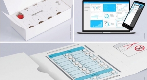
PragmatIC concept image of ready meal packaging. (Source: PragmatIC)
David Savastano, Editor10.24.18


Related Online Exclusives
-
Manufacturers News | Suppliers News

The Axia Institute and Identiv Enter Partnership
The key driver is the shared belief in joint forces and combined expertise and mutual vision to help businesses transform their supply chains.David Savastano, Editor 05.16.24
-
Conductive Inks and Coatings | Flexible and Printed Electronics | Manufacturers News | Photovoltaics | Printed Circuit Boards/Membrane Switches/In Mold Electronics | Sensors and Wearables | Smart Cards and Packaging | Suppliers News

The 2021 Conductive Ink Market
The conductive ink industry is growing with new applications on the horizon, but silver prices remain a concern.David Savastano, Editor 09.22.21
-
Breaking News | Manufacturers News | Product Releases | RFID and NFC

Identiv Introduces uCreate NFC Mobile Application Platform and Software Development Kit
The all-in-one NFC mobile application platform makes it easy to develop, prototype, test, and successfully launch NFC-enabled applications.09.02.21
-
Displays and Lighting | Flexible and Printed Electronics | Lab and Testing | Manufacturers News | Printed Circuit Boards/Membrane Switches/In Mold Electronics | Research Institutions | Sensors and Wearables | Suppliers News

DTI’s Open Innovation Test Bed is Helping Bring PE to the Market
Working with Swarovski AG on wearables, MAIER on automotive plastic parts, Grafietic on labels and ACCIONA on construction.06.30.21
-
Breaking News | RFID and NFC | Suppliers News

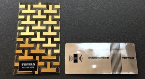
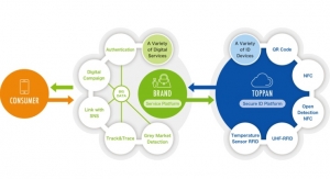
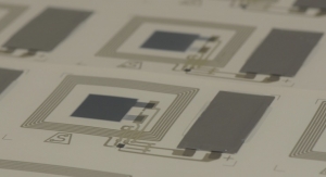
Toppan Develops Smart Packages with Built-in NFC Functions
NFC tags integrated into packaging structure enhance security, preserve design quality, and help streamline manufacturing.06.23.21
