01.04.16
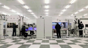
The Centre for Process Innovation (CPI) has recently partnered with NovaCentrix to install a system designed for the high speed photonic curing of printed electronics inks. The NovaCentrix PulseForge 1300 state-of-the-art system is the first of its kind in the UK to be available to clients on an open access basis, and will aid the commercialization of a host of applications including printed sensing and RFID and NFC antennas for smart packaging.
The recent installation builds upon CPI’s existing capability, allowing companies to develop and scale up concepts from laboratory scale through to pilot production.
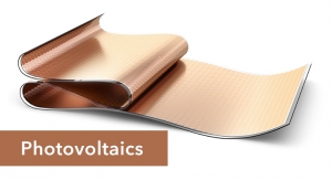
Photonic curing has become a critical process in the manufacture of printed electronics products as very little energy is needed to sinter the inks to a high temperature. This allows for printed circuits to be produced on inexpensive and flexible materials such as plastic, paper or cardboard, while achieving excellent conductivity and without causing thermal damage to these materials. The technology is ideal for a number of printed electronics-based applications that utilize low cost substrates such as printed temperature, capacitive touch and medical sensors, in addition to wearable electronics, energy harvesting devices and intelligent packaging products.
The NovaCentrix PulseForge tool at CPI uses specialist computer controlled high-intensity pulsed light technology enabling conductive inks to be sintered or annealed in a matter of milliseconds. The tool also provides the opportunity for comparably low cost inks formulated from copper-oxide and the rapid development of new printable electronics applications. Processing developed with the PulseForge 1300 at CPI can immediately be applied to volume production using the PulseForge platforms already in use for manufacturing of products sold worldwide.
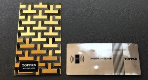
New opportunities are opening up to integrate high volume, low cost printed sensors into everyday products with applications in a number of market sectors. The Internet of Things and NFC are gathering attention from businesses, technology providers and consumers. NFC allows consumers to intuitively communicate with everyday items such as product packaging and sensors.
The printing of electronic functionality has enabled product designers to embed electronic technology into their designs, creating innovative products that are low cost, smarter, lightweight and wireless. Applications are numerous, from interactive point-of-sale products and branding to disposable printed bio-sensors used in medical analysis and unobtrusive printed smart labels that allow for identification and anti-counterfeiting control.
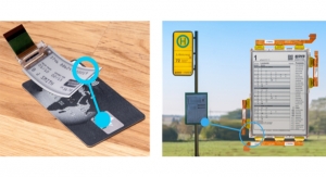
The integration of advanced printed sensors into paper and plastic opens up a wide range of market opportunities to create products with added value. Sensors can be designed to provide the opportunity to optimize logistics operations and stock control within the product life cycle, and also to indicate the validity or quality of a product or whether the packaging has been subject to tampering during its transport and storage.
“CPI is delighted to be working together with NovaCentrix to provide leading photonic curing technology for printable electronics applications,” Dr. Alan McClelland, business manager at CPI, said. “The collaboration builds upon existing printing capability at CPI, and provides the opportunity to rapidly sinter conductive inks and also assess an extensive range of functional inks and substrate materials for market testing and investment purposes.”
“CPI is well-known throughout the UK as well as internationally as a centre of excellence, especially for the development and commercialisation of printed electronics,” added Stan Farnsworth, VP marketing at NovaCentrix. “We are delighted to be able to work together with their innovative team.”
The recent installation builds upon CPI’s existing capability, allowing companies to develop and scale up concepts from laboratory scale through to pilot production.
Photonic curing has become a critical process in the manufacture of printed electronics products as very little energy is needed to sinter the inks to a high temperature. This allows for printed circuits to be produced on inexpensive and flexible materials such as plastic, paper or cardboard, while achieving excellent conductivity and without causing thermal damage to these materials. The technology is ideal for a number of printed electronics-based applications that utilize low cost substrates such as printed temperature, capacitive touch and medical sensors, in addition to wearable electronics, energy harvesting devices and intelligent packaging products.
The NovaCentrix PulseForge tool at CPI uses specialist computer controlled high-intensity pulsed light technology enabling conductive inks to be sintered or annealed in a matter of milliseconds. The tool also provides the opportunity for comparably low cost inks formulated from copper-oxide and the rapid development of new printable electronics applications. Processing developed with the PulseForge 1300 at CPI can immediately be applied to volume production using the PulseForge platforms already in use for manufacturing of products sold worldwide.
New opportunities are opening up to integrate high volume, low cost printed sensors into everyday products with applications in a number of market sectors. The Internet of Things and NFC are gathering attention from businesses, technology providers and consumers. NFC allows consumers to intuitively communicate with everyday items such as product packaging and sensors.
The printing of electronic functionality has enabled product designers to embed electronic technology into their designs, creating innovative products that are low cost, smarter, lightweight and wireless. Applications are numerous, from interactive point-of-sale products and branding to disposable printed bio-sensors used in medical analysis and unobtrusive printed smart labels that allow for identification and anti-counterfeiting control.
The integration of advanced printed sensors into paper and plastic opens up a wide range of market opportunities to create products with added value. Sensors can be designed to provide the opportunity to optimize logistics operations and stock control within the product life cycle, and also to indicate the validity or quality of a product or whether the packaging has been subject to tampering during its transport and storage.
“CPI is delighted to be working together with NovaCentrix to provide leading photonic curing technology for printable electronics applications,” Dr. Alan McClelland, business manager at CPI, said. “The collaboration builds upon existing printing capability at CPI, and provides the opportunity to rapidly sinter conductive inks and also assess an extensive range of functional inks and substrate materials for market testing and investment purposes.”
“CPI is well-known throughout the UK as well as internationally as a centre of excellence, especially for the development and commercialisation of printed electronics,” added Stan Farnsworth, VP marketing at NovaCentrix. “We are delighted to be able to work together with their innovative team.”