David Savastano, Editor03.31.16
The market for conductive inks and pastes is by all measures one of the most important success stories in the field of flexible and printed electronics. As applications continue to emerge, conductive inks are poised to grow further.
IDTechEx estimates that the market for conductive inks and pastes was more than $2.3 billion in 2015, and will grow for the foreseeable future, reaching $2.8 billion by 2020.
Dr. Khasha Ghaffarzadeh, head of consulting for IDTechEx, said that the evolving nature of the flexible and printed electronics industry is changing the nature of the conductive ink market as well, with photovoltaics and touch screens examples of segments that are shifting.
“The business dynamics in many traditional applications are changing and new areas are appearing,” said Dr. Ghaffarzadeh. “Traditionally, the largest market has been photovoltaics (PV). This market is changing. At the level of end user, solar panel production pretty much shifted entirely to China over the past five years. At the level of paste, the early group of dominant suppliers that won thanks to their product quality are losing their market share to competitors that were lower cost but are now good enough. The volume sales in this market are expanding thanks to the growth in the PV industry.
“Touch screens are another changing market,” Dr. Ghaffarzadeh added. “Conductive inks are used for printing the edge electrodes in the bezel, which are becoming thinner and thinner. The industry now wants an L/S of 20.20 so there is a need for photocurable screen inks, but long term, the use of inks for touch screens will decrease in favor of etching as even lower L/S ratios will be adopted.”
“As has been occurring over the past few years, the printed electronics market continues to grow,” said Lawrence Gasman, principal analyst for n-Tech Research. “We are seeing growth across several fields including printed circuits boards, mobile devices and the photovoltaic fields. We are also witnessing the development of applications in both the sensors and OPV fields.”
“For a few years, much of the growth in the sector was coming from solar panels, which used screenprinted silver for electrodes,” Gasman noted. “So when the solar panel industry ended its bubble period, this hurt the silver paste business. There is less growth in the solar industry these days, but the good news is that much of it is from c-Si panels, which use a lot of silver.
“There was – for a while – a lot of talk about printed gold, but the high price of industrial gold prevented a lot of applications for taking off,” Gasman added. “Gold prices have been going down, I believe, so this may be good news for gold inks and pastes.”
Roy Bjorlin, global commercial and strategic initiatives director, Electronics Materials, Sun Chemical, said there is a lot of curiosity towards electronic packaging and smart labels, and brand owners are increasingly expressing interest.
“The evolution of packaging will clearly happen across multiple verticals over time,” Bjorlin said. “However, these functionalities, ranging from consumer interaction with the package itself to collecting metrics which measure buying habits, will be adopted cautiously. Other technologies in the photovoltaics (PV) space are also gaining momentum, especially advanced PV designs both on c-Si and thin film.
“Sun Chemical’s new Advanced Materials division has developed a full range of technologies, including electronic materials specifically designed for a wide range of high speed printing processes, including screen, gravure, flexo and inkjet,” Bjorlin added. “At Sun Chemical, we view the development of advanced material solutions that fit the convertors’ manufacturing processes as essential. One specific example is our advanced nanosilver ink technology.”
Stan Farnsworth, VP of marketing for NovaCentrix, said he is seeing new opportunities emerging.
“We see interest in some of the same markets that historically have been active, including traditional flex circuits and displays,” said Farnsworth. “In the past few months though, wearables and automotive have begun to be more active.
“By far most of the applications utilizing the new materials and processing methods are still in R&D,” Farnsworth added. “We have seen some move into production, however, which is great news.”
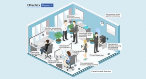
“We definitely see growth in the flexible and printed electronics market, as do many market analysts who project growth to more than double over the next 10 years,” said Doug Dixon, global marketing director, Henkel Electronic Materials LLC. “With smaller, more flexible form factors driving development for many applications – from wearables to IoT to medical and automotive – the need for capable and adaptable materials is greater than ever before.”
Leonard Allison, business manager, Engineered Materials Systems, Inc. (EMS), said that EMS is experiencing growth in printed electronics.
“Traditional membrane touch switch is holding steady as off-shore manufacturing becomes more expensive,” Allison noted. “Medical electronics and sensor applications are strong and many new applications under development will follow, but the design cycle is slow with regulations. Capacitive and proximity sensing has developed new and growing applications for both wearable technology and automotive applications.
“After many persevering years of developing new applications at the OEM level, these jobs are now in process development stage with printer contract manufacturers,” Allison added.
Dr. Daniel J. Harrison, SVP R&D for IIMAK, said that 2015 was IIMAK’s strongest year for the printed electronics segment.
“Our Metallograph Conductive Thermal Transfer Ribbon was the main contributor,” Dr. Harrison added. “Customers are using this ribbon to print RFID antennas, flex circuits, chipless RFID and other flexible electronics.”
“As has been occurring over the past few years, the printed electronics market continues to grow,” noted Dr. Fernando de la Vega, founder and CEO of PV Nano Cell. “We are seeing the scale up of PE applications. We are seeing growth across several fields, including printed circuits boards, mobile devices and the photovoltaic fields. We are also witnessing the development of applications in both the sensors and OPV fields.”
Growing Markets
While some markets are declining, other industries are emerging.
“There are many new applications,” said Dr. Ghaffarzadeh. “Printing antennas using the aerosol jet process is interesting. It deposits directly on mobile phone parts, and the advantage is a change of design no longer requires a change on tooling. This is a good market for silver nanoparticle inks.”
Dr. Ghaffarzadeh also mentioned thermoformable conductive inks, wearables and 3D printing as emerging markets.
“In-mold electronics is also becoming a good market,” said Dr. Ghaffarzadeh. “Companies print graphics and electronics on 2D sheets that are thermoformed or molded to 3D. Inks on textiles require new inks that can adhere to surfaces and can stay on for many washing cycles. 3D printed electronics embed electronic circuitry as you build layers and create things that are smart. This needs inks that cure at very low temperature, give high conductivity and adhere well, all without affecting the color of the underlying plastic.”
“We are seeing more printed electronics applications reaching pilot production and manufacturing stages,” Bjorlin said. “Some of these advanced applications are increasingly making it to the scale-up stage in the manufacturing process. Good examples include photovoltaics, such as cadmium telluride (CdTe), HIT (Heterojunction with Intrinsic Thin layer), and IBC (interdigitated back contact).”
Dixon said that while printed electronics has been touted as “the next big thing” for many years now, the technology never really moved into mainstream beyond certain applications within the automotive, medical and computing sectors.
“This may be about to change,” Dixon added. “As the wearables market begins to accelerate, more electronics are integrated into automotive applications and even display technologies become more flexible, printed electronics becomes the enabler.”
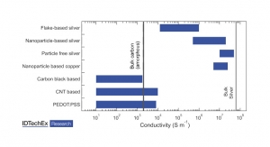
Silver nanoparticle inks remain the most common technology, with copper and carbon two other areas of note.
NANOGAP supplies both silver nanofibers and silver nanoparticles to ink formulators. Dr. Allen Reid, commercial director for NANOGAP, said he is seeing growth in the use of nanofibers.
“Nanofibers are used in screen and flexo inks for transparent conductive films,” said Dr. Reid. “We are seeing growth in lighting applications in this area. Benefits include low cost combined with good conductive and optical properties. Nanoparticles are used in conductive inkjet inks where benefits include high concentration dispersions for formulation flexibility, excellent dispersion and ink stability, combined with low temperature sintering and high conductivity.”
Dr. Reid said that NANOGAP is developing conductive nanofibers that will use half as much silver while maintaining the same level of conductivity.
“NANOGAP is finalizing the development of a new improved Nanofiber product, which will offer the same conductive properties of the current product, but at half the silver usage level,” said Dr. Reid. “Optical properties will also be improved with haze reduced from 5% to around 2%.”
“The basic materials remain the same. However, advances in pigments and particles such as nano materials are going a long way to enhance performance,” Bjorlin noted. “Sun Chemical’s pigments development and customized resins also contribute to developing next generation materials with enhanced conductivities as well as adaption to high speed printing.”
“Copper nanoparticle inks are still a little immature technology wise,” Dr. Ghaffarzadeh noted. “Carbon paste is a big area but it has a separate market to metallic inks thanks to its lower conductivity. It is used in applications like glucose strips and car seat heaters.”
“Silver variants continue to be the biggest sellers, though development of applications using alternative materials such as copper continues to be strong,” Farnsworth said.
“It’s still really about gold, silver and carbon, although there are a lot of inks made just for R&D applications,” Gasman noted. “Gold has advantages in medical and other applications where it is the fact that it does not react with other substances that is important. Silver is the most electrically conductive natural material. Carbon has been mixed with metals or used on its own for many years, and its big advantage is that it isn’t very expensive. Nano materials using these materials are also available, but mostly are used for R&D.”
Overall, Dr. Ghaffarzadeh reported that the conductive ink and paste market is growing.
“The market will change but volumes will grow. The PV market is expanding quickly, and while touch screens are diminishing, 3D antennas and others will grow,” said Dr. Ghaffarzadeh. “Sales of conductive inks were $2.3 billion in 2015 and will definitely grow.”
“It’s going to be slow unless a new applications pops up,” Gasman said. “Since the middle of the 20th century there has always been something new – appliances, computers, cell phones and then PV. It isn’t clear to me that there is something equivalent in terms of the ability to consume inks, but something in the wearables or IoT space is somewhere to look.”
“It has never been busier in my 30 years in the polymer thick film market,” Allison said. “The convergence of new IC chips, Bluetooth, data logger apps and durable printed electronics have opened the door to many exciting new applications.”
“There has been a lot of speculation about which areas will be next to start pulling in volumes of ink: incumbent applications like flexible conductors and RFID, or developing applications like wearables,” Farnsworth noted. “We see increasing activity in each, but can’t predict the future next-big-app. Our approach is to respond to all of the opportunities, not rule anything out, and to position ourselves to provide the best support possible.”
“Interest in electronic packaging is high on the list and is coming from a variety of locations,” Bjorlin said. “The US and European markets appear to be ahead of the curve. However, Sun Chemical has active projects in Japan and other Asian markets. While Touchcode technology has certainly gained a great deal of interest in many locations, other technologies, such as printed antenna for RFID and NFC systems are gaining traction and enabling smarter packaging. Printed memory is also in the headlines, but it might be slower to adopt.
“The future is bright for intelligent inks and electronic packaging,” concluded Bjorlin. “However, adoption may be slower than desired because many of the functions offered in electronics are not a natural part of the traditional converter base and continue to be somewhat cost prohibitive. It is likely that costs will drop dramatically as the traditional packaging convertor base starts developing manufacturing capabilities for electronics. For that to happen, the market also needs to determine which functions are to be implemented. This will be largely determined by a combination of cost and benefit analysis as well as consumer acceptance.”
IDTechEx estimates that the market for conductive inks and pastes was more than $2.3 billion in 2015, and will grow for the foreseeable future, reaching $2.8 billion by 2020.
Dr. Khasha Ghaffarzadeh, head of consulting for IDTechEx, said that the evolving nature of the flexible and printed electronics industry is changing the nature of the conductive ink market as well, with photovoltaics and touch screens examples of segments that are shifting.
“The business dynamics in many traditional applications are changing and new areas are appearing,” said Dr. Ghaffarzadeh. “Traditionally, the largest market has been photovoltaics (PV). This market is changing. At the level of end user, solar panel production pretty much shifted entirely to China over the past five years. At the level of paste, the early group of dominant suppliers that won thanks to their product quality are losing their market share to competitors that were lower cost but are now good enough. The volume sales in this market are expanding thanks to the growth in the PV industry.
“Touch screens are another changing market,” Dr. Ghaffarzadeh added. “Conductive inks are used for printing the edge electrodes in the bezel, which are becoming thinner and thinner. The industry now wants an L/S of 20.20 so there is a need for photocurable screen inks, but long term, the use of inks for touch screens will decrease in favor of etching as even lower L/S ratios will be adopted.”
“As has been occurring over the past few years, the printed electronics market continues to grow,” said Lawrence Gasman, principal analyst for n-Tech Research. “We are seeing growth across several fields including printed circuits boards, mobile devices and the photovoltaic fields. We are also witnessing the development of applications in both the sensors and OPV fields.”
“For a few years, much of the growth in the sector was coming from solar panels, which used screenprinted silver for electrodes,” Gasman noted. “So when the solar panel industry ended its bubble period, this hurt the silver paste business. There is less growth in the solar industry these days, but the good news is that much of it is from c-Si panels, which use a lot of silver.
“There was – for a while – a lot of talk about printed gold, but the high price of industrial gold prevented a lot of applications for taking off,” Gasman added. “Gold prices have been going down, I believe, so this may be good news for gold inks and pastes.”
Roy Bjorlin, global commercial and strategic initiatives director, Electronics Materials, Sun Chemical, said there is a lot of curiosity towards electronic packaging and smart labels, and brand owners are increasingly expressing interest.
“The evolution of packaging will clearly happen across multiple verticals over time,” Bjorlin said. “However, these functionalities, ranging from consumer interaction with the package itself to collecting metrics which measure buying habits, will be adopted cautiously. Other technologies in the photovoltaics (PV) space are also gaining momentum, especially advanced PV designs both on c-Si and thin film.
“Sun Chemical’s new Advanced Materials division has developed a full range of technologies, including electronic materials specifically designed for a wide range of high speed printing processes, including screen, gravure, flexo and inkjet,” Bjorlin added. “At Sun Chemical, we view the development of advanced material solutions that fit the convertors’ manufacturing processes as essential. One specific example is our advanced nanosilver ink technology.”
Stan Farnsworth, VP of marketing for NovaCentrix, said he is seeing new opportunities emerging.
“We see interest in some of the same markets that historically have been active, including traditional flex circuits and displays,” said Farnsworth. “In the past few months though, wearables and automotive have begun to be more active.
“By far most of the applications utilizing the new materials and processing methods are still in R&D,” Farnsworth added. “We have seen some move into production, however, which is great news.”
“We definitely see growth in the flexible and printed electronics market, as do many market analysts who project growth to more than double over the next 10 years,” said Doug Dixon, global marketing director, Henkel Electronic Materials LLC. “With smaller, more flexible form factors driving development for many applications – from wearables to IoT to medical and automotive – the need for capable and adaptable materials is greater than ever before.”
Leonard Allison, business manager, Engineered Materials Systems, Inc. (EMS), said that EMS is experiencing growth in printed electronics.
“Traditional membrane touch switch is holding steady as off-shore manufacturing becomes more expensive,” Allison noted. “Medical electronics and sensor applications are strong and many new applications under development will follow, but the design cycle is slow with regulations. Capacitive and proximity sensing has developed new and growing applications for both wearable technology and automotive applications.
“After many persevering years of developing new applications at the OEM level, these jobs are now in process development stage with printer contract manufacturers,” Allison added.
Dr. Daniel J. Harrison, SVP R&D for IIMAK, said that 2015 was IIMAK’s strongest year for the printed electronics segment.
“Our Metallograph Conductive Thermal Transfer Ribbon was the main contributor,” Dr. Harrison added. “Customers are using this ribbon to print RFID antennas, flex circuits, chipless RFID and other flexible electronics.”
“As has been occurring over the past few years, the printed electronics market continues to grow,” noted Dr. Fernando de la Vega, founder and CEO of PV Nano Cell. “We are seeing the scale up of PE applications. We are seeing growth across several fields, including printed circuits boards, mobile devices and the photovoltaic fields. We are also witnessing the development of applications in both the sensors and OPV fields.”
Growing Markets
While some markets are declining, other industries are emerging.
“There are many new applications,” said Dr. Ghaffarzadeh. “Printing antennas using the aerosol jet process is interesting. It deposits directly on mobile phone parts, and the advantage is a change of design no longer requires a change on tooling. This is a good market for silver nanoparticle inks.”
Dr. Ghaffarzadeh also mentioned thermoformable conductive inks, wearables and 3D printing as emerging markets.
“In-mold electronics is also becoming a good market,” said Dr. Ghaffarzadeh. “Companies print graphics and electronics on 2D sheets that are thermoformed or molded to 3D. Inks on textiles require new inks that can adhere to surfaces and can stay on for many washing cycles. 3D printed electronics embed electronic circuitry as you build layers and create things that are smart. This needs inks that cure at very low temperature, give high conductivity and adhere well, all without affecting the color of the underlying plastic.”
“We are seeing more printed electronics applications reaching pilot production and manufacturing stages,” Bjorlin said. “Some of these advanced applications are increasingly making it to the scale-up stage in the manufacturing process. Good examples include photovoltaics, such as cadmium telluride (CdTe), HIT (Heterojunction with Intrinsic Thin layer), and IBC (interdigitated back contact).”
Dixon said that while printed electronics has been touted as “the next big thing” for many years now, the technology never really moved into mainstream beyond certain applications within the automotive, medical and computing sectors.
“This may be about to change,” Dixon added. “As the wearables market begins to accelerate, more electronics are integrated into automotive applications and even display technologies become more flexible, printed electronics becomes the enabler.”
Silver nanoparticle inks remain the most common technology, with copper and carbon two other areas of note.
NANOGAP supplies both silver nanofibers and silver nanoparticles to ink formulators. Dr. Allen Reid, commercial director for NANOGAP, said he is seeing growth in the use of nanofibers.
“Nanofibers are used in screen and flexo inks for transparent conductive films,” said Dr. Reid. “We are seeing growth in lighting applications in this area. Benefits include low cost combined with good conductive and optical properties. Nanoparticles are used in conductive inkjet inks where benefits include high concentration dispersions for formulation flexibility, excellent dispersion and ink stability, combined with low temperature sintering and high conductivity.”
Dr. Reid said that NANOGAP is developing conductive nanofibers that will use half as much silver while maintaining the same level of conductivity.
“NANOGAP is finalizing the development of a new improved Nanofiber product, which will offer the same conductive properties of the current product, but at half the silver usage level,” said Dr. Reid. “Optical properties will also be improved with haze reduced from 5% to around 2%.”
“The basic materials remain the same. However, advances in pigments and particles such as nano materials are going a long way to enhance performance,” Bjorlin noted. “Sun Chemical’s pigments development and customized resins also contribute to developing next generation materials with enhanced conductivities as well as adaption to high speed printing.”
“Copper nanoparticle inks are still a little immature technology wise,” Dr. Ghaffarzadeh noted. “Carbon paste is a big area but it has a separate market to metallic inks thanks to its lower conductivity. It is used in applications like glucose strips and car seat heaters.”
“Silver variants continue to be the biggest sellers, though development of applications using alternative materials such as copper continues to be strong,” Farnsworth said.
“It’s still really about gold, silver and carbon, although there are a lot of inks made just for R&D applications,” Gasman noted. “Gold has advantages in medical and other applications where it is the fact that it does not react with other substances that is important. Silver is the most electrically conductive natural material. Carbon has been mixed with metals or used on its own for many years, and its big advantage is that it isn’t very expensive. Nano materials using these materials are also available, but mostly are used for R&D.”
Overall, Dr. Ghaffarzadeh reported that the conductive ink and paste market is growing.
“The market will change but volumes will grow. The PV market is expanding quickly, and while touch screens are diminishing, 3D antennas and others will grow,” said Dr. Ghaffarzadeh. “Sales of conductive inks were $2.3 billion in 2015 and will definitely grow.”
“It’s going to be slow unless a new applications pops up,” Gasman said. “Since the middle of the 20th century there has always been something new – appliances, computers, cell phones and then PV. It isn’t clear to me that there is something equivalent in terms of the ability to consume inks, but something in the wearables or IoT space is somewhere to look.”
“It has never been busier in my 30 years in the polymer thick film market,” Allison said. “The convergence of new IC chips, Bluetooth, data logger apps and durable printed electronics have opened the door to many exciting new applications.”
“There has been a lot of speculation about which areas will be next to start pulling in volumes of ink: incumbent applications like flexible conductors and RFID, or developing applications like wearables,” Farnsworth noted. “We see increasing activity in each, but can’t predict the future next-big-app. Our approach is to respond to all of the opportunities, not rule anything out, and to position ourselves to provide the best support possible.”
“Interest in electronic packaging is high on the list and is coming from a variety of locations,” Bjorlin said. “The US and European markets appear to be ahead of the curve. However, Sun Chemical has active projects in Japan and other Asian markets. While Touchcode technology has certainly gained a great deal of interest in many locations, other technologies, such as printed antenna for RFID and NFC systems are gaining traction and enabling smarter packaging. Printed memory is also in the headlines, but it might be slower to adopt.
“The future is bright for intelligent inks and electronic packaging,” concluded Bjorlin. “However, adoption may be slower than desired because many of the functions offered in electronics are not a natural part of the traditional converter base and continue to be somewhat cost prohibitive. It is likely that costs will drop dramatically as the traditional packaging convertor base starts developing manufacturing capabilities for electronics. For that to happen, the market also needs to determine which functions are to be implemented. This will be largely determined by a combination of cost and benefit analysis as well as consumer acceptance.”