
Anthony Locicero, Associate Editor03.09.18
There are several promising avenues for flexible and printed electronics manufacturers to explore, according to equipment industry experts.
For example, XENON Corporation CEO Lou Panico pointed to semiconductors and hybrid circuits along with display manufacturing.
Nicolas Bernardin, CERADROP deputy marketing manager, said his company is serving development markets “in hope that they will also move towards production paths much like the flexible and foldable OLED and QLED (quantum dot LED) displays and lighting markets.”
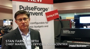
NovaCentrix has seen a lot of growth in the exploration of materials in the automotive market, according to chief marketing officer Stan Farnsworth. But there’s also a growth in wearables and medical devices, he said. “I would say this is a result of a need for thinner, lighter, flexible, inexpensive, consumable parts in these application areas,” Farnsworth added.
Optomec’s Mike O’Reilly offered up a four-part response:
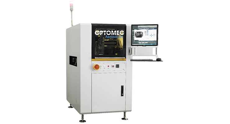
Printed 3D interconnects: “Direct printing of conformal 3D interconnects as an alternative to wire-bonding provides wide-ranging benefits, including smaller footprint, lower package height, reduced crosstalk and improved mechanical reliability,” the director of Aerosol Jet product management said. “The Aerosol Jet solution can produce interconnect traces as narrow as 25 micron to support pad pitches down to 50 micron, and the solution is applicable to direct die attach and die stack applications, i.e. combining dedicated memory with processor.”
Component and die attach: “With its unique ability to print fine features with high viscosity conductive inks, the Aerosol Jet HD platform can produce high resolution adhesive pads with features as small as 25 micron,” O’Reilly said. “This supports conductive attach of today’s smallest die and components, without the need for manual re-work increasing overall throughput and eliminating wasteful end-of-line clean-up steps.”
Printed dielectrics, insulators, and adhesives: “In addition to conductive materials, Aerosol Jet is capable of high resolution printing of a wide range of common non-conductive electronics materials,” he said. “Applications include MEMS bonding, seal rings, local passivation, and insulative overcoats. When coupled with conductor printing, Aerosol Jet can produce high density cross-over circuits, reducing the number of layers and feed-throughs in multi-layer circuitry/PCBs.
Chip and board level shielding: “Aerosol Jet HD platform is capable of producing precision conformal coatings on non-planar surfaces, enabling chip and board level EMI shielding that are requisite for today’s mobile devices. Larger nozzles enable single pass printing of coatings measuring from millimeters to centimeters in width, while maintaining uniform layer thickness from 100nm to tens of microns,” he added. “Couple this capability with Aerosol Jet’s fine feature printing and edge coatings of complex packages, selective exposure to contacts and ground planes is now possible. This is a large advancement for open atmosphere coating applications.”
Has there been a shift to larger production volumes and/or commercialization? The answer to that question varies.
Panico said the march to volume commercialization has moved “painfully slow.”
“Yes, OLED has been a market success, but is perhaps not the best model for other application segments,” the CEO noted. “Too many promises of accelerated market success may have actually pushed projects aside that require a longer development cycle. Seeking almost overnight commercialization may have been harmful, but has provided initial lessons. We are seeing highly innovative new application ideas that are focusing on retail consumer and industrial areas spanning global markets.”
O’Reilly said that Optomec is seeing orders from companies for multiple systems as well as new equipment orders “that are addressing next generation printed electronic products and associated manufacturing challenges.”
Large display companies are moving towards pilot production of inkjet printing of OLED mobile displays, according to Bernardin. “They are developing larger QLED displays with inkjet production equipment consideration,” he added.
In other inkjet production areas of sensors and smart packaging, CERADROP is only seeing press releases detailing collaborations and topics, Bernardin said. “We have not seen growth numbers in this segment yet,” he added.
Many of NovaCentrix’s customers are still in the development and validation process, Farnsworth said, but the company has seen some clientele “move forward and implement full-scale production.
“The trend we are noticing is that increasingly the customers are needing assistance in incorporating the technologies into their products,” Farnsworth continued. “At our recent exhibition at CES in Las Vegas – one of the largest consumer electronics conferences in the world – we noticed a larger interest in integrating existing technologies with printed electronics technologies. Many companies are realizing they have a need for manufacturing more modern electronics, with conformability or improved simplified manufacturing, and aren’t quite sure how to yet accomplish this with their products. There is a higher recognition for printed electronics and the capabilities that come with having printed electronics parts.”
Recent Innovations
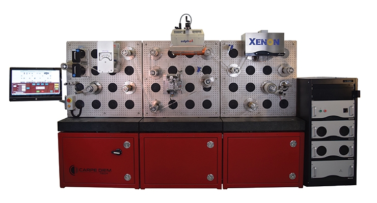
At Printed Electronics USA 2017, XENON debuted the Centauri, a joint venture with Carpe Diem Technologies that provides a complete R2R solution for PE sintering.
“Centauri has enabled many customers to quickly customize pilot systems for proof-of-principle. It has also assisted us to better understand the over-all nature of the PE manufacturing process and the most pressing issues facing our customers,” Panico said. “Our introduction of the industry’s lowest cost, high intensity, benchtop sintering system, model X-1100, has provided customers with a development tool that helps them optimize their overall PE process faster and more effectively.
“Photonic curing has been a challenge for many manufactures whose expertise lies in other aspects of the PE process,” he continued. “With the X-1100 in-house development system and other XENON sintering systems, their ability to quickly learn how this tool is applied for their unique applications has been and continues to be, accelerated.”
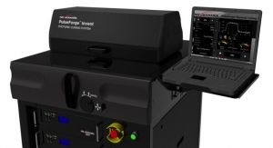
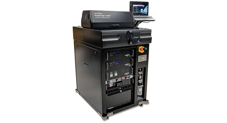
At the same show, NovaCentrix unveiled its PulseForge Invent.
“The PulseForge Invent was designed to meet the need of our customers in the academic and R&D areas,” Farnsworth said. “For many, printed electronics is still an exploratory area that requires a lot of research and development in their products, so we developed a state-of-the-art PulseForge platform with a lower base cost of just $59,000. This system is fully configurable to meet the growing needs of our customers as they move forward in their research and require a higher power system.”
Per O’Reilly, Optomec has developed a new generation of Aerosol Jet print solutions – spanning from R&D to production requirements.
“From our closely coupled, interchangeable material cassette solutions for integration with standard third party dispense platforms, to our own Optomec Aerosol Jet HD Systems, product evolution has been driven through collaboration with our current production-oriented customers,” he said. “We have further developed production ready material process recipes that help our customers expedite production ready equipment installations and start-up.”
Bernardin said that CERADROP is still moving towards “realization for promising OLED lighting in smart packaging applications.”
But for the past decade, the company has been “serving the inkjet deposition global development communities to [develop] commercialized inkjet digital non-contact deposition processes, environmentally friendly inks, and ink consumption methods at high resolution and high throughput.”
For example, XENON Corporation CEO Lou Panico pointed to semiconductors and hybrid circuits along with display manufacturing.
Nicolas Bernardin, CERADROP deputy marketing manager, said his company is serving development markets “in hope that they will also move towards production paths much like the flexible and foldable OLED and QLED (quantum dot LED) displays and lighting markets.”
NovaCentrix has seen a lot of growth in the exploration of materials in the automotive market, according to chief marketing officer Stan Farnsworth. But there’s also a growth in wearables and medical devices, he said. “I would say this is a result of a need for thinner, lighter, flexible, inexpensive, consumable parts in these application areas,” Farnsworth added.
Optomec’s Mike O’Reilly offered up a four-part response:
Printed 3D interconnects: “Direct printing of conformal 3D interconnects as an alternative to wire-bonding provides wide-ranging benefits, including smaller footprint, lower package height, reduced crosstalk and improved mechanical reliability,” the director of Aerosol Jet product management said. “The Aerosol Jet solution can produce interconnect traces as narrow as 25 micron to support pad pitches down to 50 micron, and the solution is applicable to direct die attach and die stack applications, i.e. combining dedicated memory with processor.”
Component and die attach: “With its unique ability to print fine features with high viscosity conductive inks, the Aerosol Jet HD platform can produce high resolution adhesive pads with features as small as 25 micron,” O’Reilly said. “This supports conductive attach of today’s smallest die and components, without the need for manual re-work increasing overall throughput and eliminating wasteful end-of-line clean-up steps.”
Printed dielectrics, insulators, and adhesives: “In addition to conductive materials, Aerosol Jet is capable of high resolution printing of a wide range of common non-conductive electronics materials,” he said. “Applications include MEMS bonding, seal rings, local passivation, and insulative overcoats. When coupled with conductor printing, Aerosol Jet can produce high density cross-over circuits, reducing the number of layers and feed-throughs in multi-layer circuitry/PCBs.
Chip and board level shielding: “Aerosol Jet HD platform is capable of producing precision conformal coatings on non-planar surfaces, enabling chip and board level EMI shielding that are requisite for today’s mobile devices. Larger nozzles enable single pass printing of coatings measuring from millimeters to centimeters in width, while maintaining uniform layer thickness from 100nm to tens of microns,” he added. “Couple this capability with Aerosol Jet’s fine feature printing and edge coatings of complex packages, selective exposure to contacts and ground planes is now possible. This is a large advancement for open atmosphere coating applications.”
Has there been a shift to larger production volumes and/or commercialization? The answer to that question varies.
Panico said the march to volume commercialization has moved “painfully slow.”
“Yes, OLED has been a market success, but is perhaps not the best model for other application segments,” the CEO noted. “Too many promises of accelerated market success may have actually pushed projects aside that require a longer development cycle. Seeking almost overnight commercialization may have been harmful, but has provided initial lessons. We are seeing highly innovative new application ideas that are focusing on retail consumer and industrial areas spanning global markets.”
O’Reilly said that Optomec is seeing orders from companies for multiple systems as well as new equipment orders “that are addressing next generation printed electronic products and associated manufacturing challenges.”
Large display companies are moving towards pilot production of inkjet printing of OLED mobile displays, according to Bernardin. “They are developing larger QLED displays with inkjet production equipment consideration,” he added.
In other inkjet production areas of sensors and smart packaging, CERADROP is only seeing press releases detailing collaborations and topics, Bernardin said. “We have not seen growth numbers in this segment yet,” he added.
Many of NovaCentrix’s customers are still in the development and validation process, Farnsworth said, but the company has seen some clientele “move forward and implement full-scale production.
“The trend we are noticing is that increasingly the customers are needing assistance in incorporating the technologies into their products,” Farnsworth continued. “At our recent exhibition at CES in Las Vegas – one of the largest consumer electronics conferences in the world – we noticed a larger interest in integrating existing technologies with printed electronics technologies. Many companies are realizing they have a need for manufacturing more modern electronics, with conformability or improved simplified manufacturing, and aren’t quite sure how to yet accomplish this with their products. There is a higher recognition for printed electronics and the capabilities that come with having printed electronics parts.”
Recent Innovations
At Printed Electronics USA 2017, XENON debuted the Centauri, a joint venture with Carpe Diem Technologies that provides a complete R2R solution for PE sintering.
“Centauri has enabled many customers to quickly customize pilot systems for proof-of-principle. It has also assisted us to better understand the over-all nature of the PE manufacturing process and the most pressing issues facing our customers,” Panico said. “Our introduction of the industry’s lowest cost, high intensity, benchtop sintering system, model X-1100, has provided customers with a development tool that helps them optimize their overall PE process faster and more effectively.
“Photonic curing has been a challenge for many manufactures whose expertise lies in other aspects of the PE process,” he continued. “With the X-1100 in-house development system and other XENON sintering systems, their ability to quickly learn how this tool is applied for their unique applications has been and continues to be, accelerated.”
At the same show, NovaCentrix unveiled its PulseForge Invent.
“The PulseForge Invent was designed to meet the need of our customers in the academic and R&D areas,” Farnsworth said. “For many, printed electronics is still an exploratory area that requires a lot of research and development in their products, so we developed a state-of-the-art PulseForge platform with a lower base cost of just $59,000. This system is fully configurable to meet the growing needs of our customers as they move forward in their research and require a higher power system.”
Per O’Reilly, Optomec has developed a new generation of Aerosol Jet print solutions – spanning from R&D to production requirements.
“From our closely coupled, interchangeable material cassette solutions for integration with standard third party dispense platforms, to our own Optomec Aerosol Jet HD Systems, product evolution has been driven through collaboration with our current production-oriented customers,” he said. “We have further developed production ready material process recipes that help our customers expedite production ready equipment installations and start-up.”
Bernardin said that CERADROP is still moving towards “realization for promising OLED lighting in smart packaging applications.”
But for the past decade, the company has been “serving the inkjet deposition global development communities to [develop] commercialized inkjet digital non-contact deposition processes, environmentally friendly inks, and ink consumption methods at high resolution and high throughput.”